Several megatrends are shaping contemporary digital society, and these in turn are driving the continuous development and expanding capabilities of lithographic patterning equipment for semiconductor manufacturing.
2D-IC density scaling is beginning to reach its cost limits, particularly in the case of patterning processes. As these limits are reached, advances in miniaturization and device performance continue to extend towards 3D integration and heterogeneous integration (HI) within advanced packaging.
This novel approach is regarded as a central factor in the development of next-generation devices, whereby the advent of mobile processors has prompted an initial growth cycle in 3D/HI. It is anticipated that this growth cycle will continue as high-performance applications such as 5G and artificial intelligence (AI) become more commonplace in mobile devices. Other drivers include megatrends such as autonomous driving and the Internet of Things (IoT), both of which require high reliability and data network capacity.
Over the years, advanced packaging technologies have become more complex and varied, with 3D integration enabling a shift from single to multi-die packaging. This is just one example of addressing the challenge of managing the substantial amounts of data generated by high-performance computing.
Continuous innovation in chiplet design coupled with an ever-expanding range of integration schemes (either on silicon, embedded, or in package) may now include several patterning levels. Design flexibility has become increasingly important, and the industry now demands shorter development cycles along with the ability to accommodate a wide range of advanced packaging platforms simultaneously. This has necessitated the adoption of both die and wafer-level designs simultaneously during back-end lithographic processing.
Any advanced product design mix will add multiple masking levels, meaning that masks and mask inventory/cleanroom storage represent a considerable fraction of overall production costs. Replacement parts for conventional laser sources or Hg lamps may also incur high costs.
Wait times for new physical mask sets and complex proof-of-new-design concepts for high product-mix designs can result in prolonged development cycles when working in conventional mask-based production environments.
These critical needs in semiconductor packaging have prompted the development of EVG’s maskless exposure (MLE™) technology. MLE™ technology offers design flexibility while simultaneously enabling unique scalability in both development and production facilities, reducing development cycles between the R&D and production phase through the elimination of consumable costs and mask-related difficulties.
This novel technology offers high-resolution (<2 µm L/S), stitch-free, and dynamically addressable exposure of the entire substrate surface, therefore enabling agile processing and ensuring low cost of ownership (CoO).
Limitations of Traditional Exposure Methods
The resolution of any optical imaging system is fundamentally defined by the ratio of exposure wavelength and its numerical aperture (NA). NA determines the light-gathering and light-emitting potential through the lens, which is characterized by the angle of aperture and therefore dependent on focal length.
Alteration of NA in exposure systems is technically more cost effective than shortening the light source’s UV wavelength. Imaging exposure systems like steppers are generally driven towards higher NA, thus enabling structuring of finer critical dimensions.
Conversely, higher NA will reduce the depth of focus. It is therefore important to find a balance between resolution and focal depth in terms of the interconnect circuit design. This is essential in advanced packaging, because the reconstitution of wafers is a central factor in integrating die from different wafer manufacturers in a multi-die solution.
As well as the aforementioned physical limitations, further difficulties arise due to inaccuracies from the variations in die placement and die shift caused by over-molding. Current lithography steppers and other mask-based systems often struggle to manage these difficulties.
The given reticle size and optical dimensions of static exposure systems result in limits to the exposure area. This can be especially challenging when working with larger die interposer fabrication, because stitch lines or mismatched overlap regions of reticle exposure fields have the potential to adversely affect electrical properties within the redistribution layer (RDL).
When working with advanced devices with the complex layouts needed for advanced graphics processing, high-performance computing (HPC) and AI, it is important to be able to generate a stitch-less pattern for interposers that exceeds the size of current reticles.
MLE™ meets these needs via a distinct combination of sub-nanometer range stage motion accuracy, real time patterning of a vector-based mask file and powerful, distortion-free, high-intensity optics. Other approaches that must rasterize the mask image before patterning will generate approximately 141 GB of data for each 300 mm wafer.
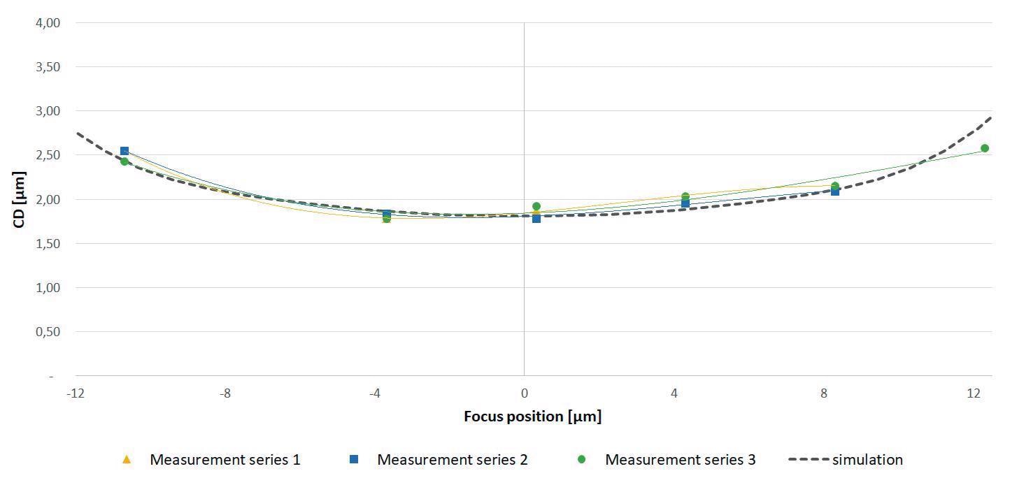
Figure 1. Critical dimension versus focus position for DoF process window evaluation. Image Credit: EV Group
The digital mask pattern is projected onto the substrate surface with sub-µs timing accuracy. The MLE™ imaging system is diffraction-limited, much like the majority of modern lenses. It supports a depth of focus (DoF) of ±12 µm. Figure 1 shows a measurement of the DoF process window performance at 2 µm L/S along with the simulated curve.
The usable dynamic focused range is extended to more than 100 µm thanks to the exposure window, the relatively small exposure field and the <1 µm precise autofocus. Bowed and warped substrates can be easily compensated for due to the system’s ability to control the focus position on a larger scale of the wafer position via chuck positioning and wafer clamping.
Dynamic Exposure Methods and Active Die-Shift Compensation
Current back-end lithographic systems are unable to control distortions that are smaller than the exposure field. These systems will therefore struggle with non-linear, high-order substrate distortions and die-shift-related issues, particularly following die reconstitution on the wafer.
To adapt to surface variations and the substrate material, MLE™ utilizes dynamic alignment modes with an automatic focus. Advanced distortion functionality relates and analyzes real-time data from synchronized visible or near-infrared topside and backside alignment. It achieves this by actively compensating for mechanical die placement, high-order distortions of the substrate and other stress-induced inaccuracies such as rotation, displacement, and expansion.
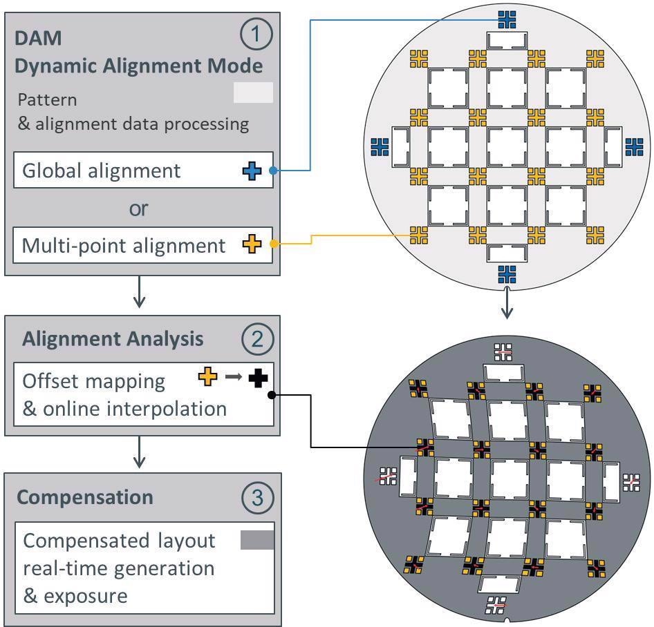
Figure 2. Advanced distortion compensation schematic process flow. Image Credit: EV Group
Figure 2 provides a visualization of the process flow of the advanced distortion correction function and dynamic alignment modes. Dynamic alignment features global and multi-point wafer alignment options, typically enabling up to 16 alignment marks (marked with blue and yellow) to be randomly placed in the layout. This allows the instrument to comprehensively cover the most critical areas on the substrate while also compensating for global distortions.
Once misalignment measurement has been completed, displacement vectors will be further compiled in parallel prior to the design being interpolated and rendered in real-time. These exposed patterns will be fully error compensated without inducing overlapping or non-covered regions, therefore ensuring minimal misalignment with no impact on the throughput of the patterning process.
The example shown here presents a visualization of a compensated layout (dark grey) following an extreme atypical misalignment (indicated with red arrows). This is a result of compensating the actual position of 16 marks (yellow) of multi-point alignment using the dynamic alignment mode.
When working with bonded, opaque substrates or other non-transparent materials common in multi-layer and multi-die processing, backside alignment will play a considerable role. Referencing the same structure for multiple exposures will also help minimize misalignment as the density of current pattern design increases.
Overlay errors or any kind of misalignment will affect the electrical properties of contacts and insulation, and these may also result in connection failures that significantly impact fab yield, CoO, and overall productivity.
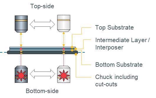
Figure 3. Schematic drawing of top and bottom-side alignment objectives. Image Credit: EV Group
Systems fitted with MLE™ technology generally integrate full wafer backside alignment (Figure 3), employing dedicated objectives with near IR capability and proprietary chuck design to accommodate wafer sizes up to 300 mm.
Die distortion errors induced after reconstitution on the wafer are typical when working with FOWLP. In these cases, advanced distortion functionality should be applied at the die level, with active compensation and rerouting results relying solely on external metrology data.
Distortion compensation algorithms will typically include mathematical correction of scale, rotation, shear, and translation (shift). When addressing die-placement-error compensation, the model will limit distortions within the dies to the rigid body of the die. This is generally represented by two (external) alignment points per die.
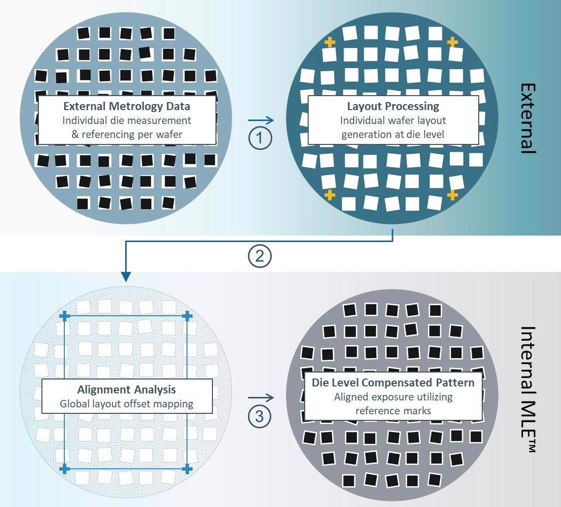
Figure 4. Die-level compensation schematic process flow. Image Credit: EV Group
The immediacy of the conversion process means that dynamic binary pattern generation will complement externally acquired metrology data for each die. This is done individually per substrate just prior to exposure, in order to compensate for overlay/positioning errors resulting from handling or pre-processing excluding potential thermal influences. Figure 4 visualizes a simplified data integrity flow of die-level compensation.
MLE™ patterning facilitates the real-time individualized wafer-level layouts and simultaneous structuring of individual die layouts. This is particularly useful when working with ad hoc die annotations, functional and directly readable encryption codes, serial numbers, active fuse map patterning to optimize device binning for process, or device tracking and documentation. This will also ultimately lead to improved overall yield.
Programmable modulations of UV dosage at the sub-pixel level allow the use of exposure gradients. These are used for controlled resist-thickness-level variations following the development process - also known as greyscale lithography. This approach effectively facilitates the fabrication of complex 3D multi-level resist patterns highly suited to multiple patterning processes, MEMS devices, dual damascene, and both refractive and diffractive micro-optical elements.
The digital programmable die/wafer layout may be stored in a range of industry standard layout design file formats; for example, Gerber, GDSII, Oasis, ODB++, or BMP. Because the layout is computationally processed on the system under recipe control, factors such as resist type (positive/negative), exposure dose level, or design layout complexity will not impact the speed of the patterning process.
Patterning Modularity and Vital Positioning in Sub-Grid
MLE’s resolution makes it suitable for typical back-end-of-line resolutions with fine control of the irradiated lines, as well as their gaps (L/S <2 µm). It can accommodate these resolutions while maintaining CD uniformity (CDU <10% CD) and positional accuracy of any arbitrary structures present in a 248 nm patterning grid scale.
Distortion-free optics and stage placement accuracy help to ensure seamless projection across the whole substrate. The exposure may be conducted with highly flexible intensity control and precise light-source-spectrum tuning. These factors allow users to achieve optimal absorption and reliable processing when working with a wide range of commercially available and novel photoresists.
The exposure light source functions at a wavelength spectrum of 375 nm and 405 nm. This facilitates a mix and match approach, using wavelengths to mimic known-good-process recipes (for example, to follow the traditional mercury lamp spectrum) or to customize the exposure according to specific customer demands.
It is possible to apply both wavelengths simultaneously to any arbitrary mixture, enabling thin-resist patterning including positive, negative, patternable dielectrics, polyimide, dry film or even PCB materials. It is also possible to support thick resist exposures at high aspect ratios, such as those commonly found in wafer-level packaging, microfluidics, 3D MEMS patterning, and integrated photonics applications.
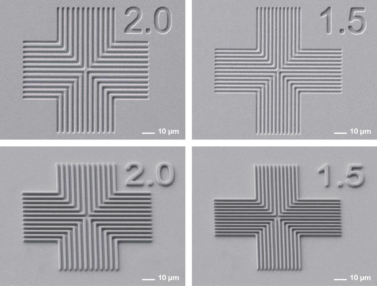
Figure 5. SEM results collage: Line space resolution tests on 1 μm thick positive AZ MIR 701 (top), Line space resolution tests on 2 μm thick negative AZ nLOF (bottom). Image Credit: EV Group
Figure 5 (top) includes a number of SEM images showing standard line-space resolution targets on 1 µm thick positive AZ MIR 701 resist. Figure 5 (bottom) shows line-space resolution tests on 2 µm thick negative tone resist AZ nLOF. In each case, a 1.5 µm L/S result was achieved via additional process optimization.
This optimization involved the reduction of surface reflection effects, achieved through the application of anti-reflective coatings or the modification of substrate material properties.
The MLE™ technology can also be used to finely control depth of focus (DoF), order achieving steep sidewalls and therefore maintaining the desired 3D contour of the resist, preventing edge topping or avoiding footing. Significant working distance coupled with automatic adaptive focus help ensure patterning uniformity across the exposure surface.
In order to demonstrate a range of line and spacing patterning performance, as well as sidewall patterning quality, a commonly utilized TOK P-W1000T resist for fine-line and core-line RDL creation was selected.
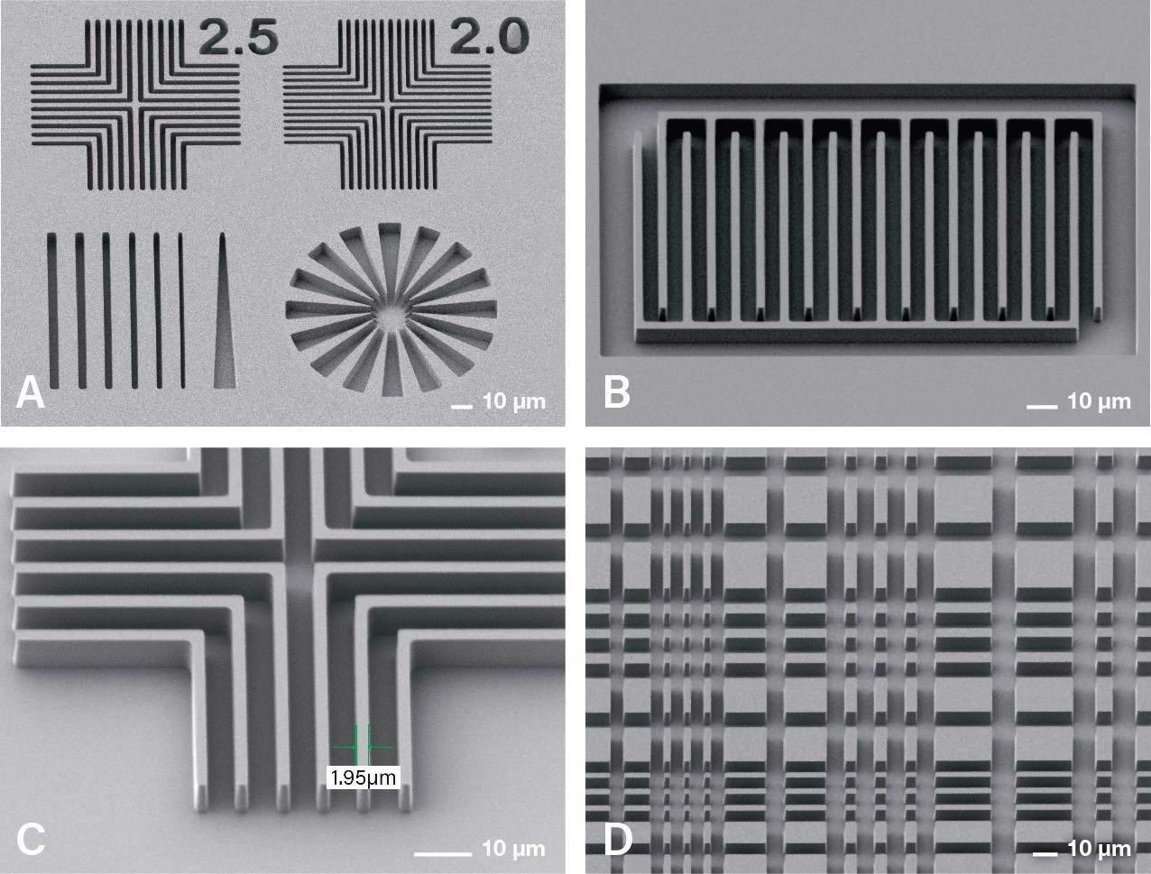
Figure 6. Baseline evaluation on (A) 8 μm thick TOK P-W1000T, (B) meander with 5 μm L/S, (C) 1:2 spacing variation, (D) L/S variation in both horizontal and vertical directions with ratios of 1:1, 1:2, 1:3, 1:4. Image Credit: EV Group
Figure 6 displays a number of examples of SEM images of baseline evaluation, demonstrating:
- 2 µm L/S resolution targeted on 8 µm film thickness
- 5 µm L/S resolution with meander pattern
- Spacing variation of 1:2 ratio
- L/S variation in both horizontal and vertical directions with ratios of 1:1, 1:2, 1:3, 1:4.
Maskless Operation Scalability
Back-end lithography results achieved during R&D via direct imaging equipment have historically lacked the technological resilience to properly function with high-volume-manufacturing (HVM) lines fitted with steppers. The industry is seeing an ever-expanding product mix – for example, chiplets and segmented dies – and this is proving to be a driver for continued performance scaling and increasing variability of applications.
These factors have prompted an increasing need for dynamic patterning at various resist thicknesses and dose levels. MLE™ can provide a high DoF at 2 µm production resolution, effectively leveraging the physical diffraction limit established by the optics.
MLE™ is also highly scalable, with its modular system scaling according to user needs through the addition of UV exposure heads (Figure 7). This facilitates a rapid transition from R&D to HVM mode, effectively accommodating throughput optimization, or adaptation to different substrate sizes and materials. MLE™ is ideal for processing a range of substrates ranging from small silicon or compound semiconductor wafers up to panel sizes.
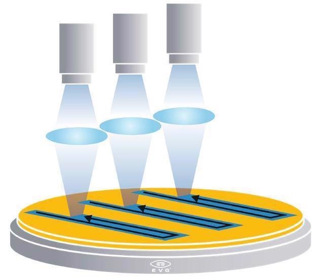
Figure 7. MLE’s unique clustered exposure configuration enables exposure heads to be easily added to adjust for different throughput needs and substrate sizes. Image Credit: EV Group
Summary
MLE™ technology provides a novel approach to patterning, offering smart and agile digital processing and delivering a consumable-free infrastructure and maskless scalability in terms of throughput and format.
MLE™ can achieve the same high patterning performance regardless of photoresist. It achieves this thanks to a flexible, reliable and scalable high-power UV laser source combination that can accommodate multiple wavelength options.
The platform facilitates patterning of a wide range of materials using the same optics; for example, silicon, glass, mold, polymers and laminates. The wafer chuck and autofocus system can compensate for substrate bow and warp, an especially important consideration in applications such as FOWLP.
The technology provides virtually unlimited design flexibility, opening up the currently conservative environment to new innovations, helping to shorten development cycles, and bridging the gap between R&D and HVM.
Acknowledgments
Produced from materials originally authored by Bozena Matuskova, Boris Považay, Frank Bögelsack, Roman Holly, Tobias Zenger, Thomas Uhrmann, and Bernhard Thallner from EV Group.
This information has been sourced, reviewed and adapted from materials provided by EV Group.

EV Group (EVG) is a leading supplier of high-volume production equipment and process solutions for the manufacture of semiconductors, MEMS, compound semiconductors, power devices and nanotechnology devices.
A recognized market and technology leader in wafer-level bonding and lithography for advanced packaging and nanotechnology, EVG’s key products include wafer bonding, thin-wafer processing and lithography/nanoimprint lithography (NIL) equipment, photoresist coaters, as well as cleaning and inspection/metrology systems.
With state-of-the-art application labs and cleanrooms at its headquarters in Austria, as well as in the U.S. and Japan, EVG is focused on delivering superior process expertise to its global R&D and production customer and partner base – from the initial development through to the final integration at the customer’s site.
Founded in 1980, EVG services and supports an elaborate network of global customers and partners all over the world, with more than 1000 employees worldwide and fully-owned subsidiaries in the U.S., Japan, South Korea, China and Taiwan.
For more information on this source, please visit EV Group.