Current silicon semiconductors can be as small as 20 nm in size, making them an ideal option for fast computing using minimal energy.
Technology at the nanoscale has both advantages and disadvantages. Its minuscule features can pose challenges for quality control, requiring high levels of magnification to accurately examine.
This level of magnification can be achieved using electron microscopy, but external perturbations, like vibrations and external magnetic fields, must be mitigated in order to attain the level of accuracy required.
Quality Control Using Electron Microscopes
Manufacturing smaller semiconductors increase computing speeds because the electrons have a shorter path to travel, allowing information to be sent more rapidly. This shorter path also results in less heat being generated in the wires, decreasing overall energy loss.
However, these small components are difficult to check for defects. High accuracy and large magnification are required, making electron microscopes the only viable instruments for this task.
Electron microscopes are capable of several million times magnification and are able to distinguish features nanometres in size, presuming the electron beam is positioned appropriately.
Magnification capacity greatly depends on the instrument itself, but this can also be affected by acoustic waves, vibrations and stray magnetic fields. It is therefore imperative that an electron microscope is protected from external disturbances to ensure good image quality.
Detection of Magnetic Fields and Their Origin
External magnetic fields may stem from a range of sources.
For example, AC fields with frequencies around 60 Hz may be caused by other instruments in the lab, while DC disturbances may be triggered by changes in the Earth’s magnetic field or generated by the movement of ferromagnetic objects, such as metal elevators and doors.
These types of fields affect the image in different ways: AC fields appear as jagged lines, while DC fields result in wavy features.
Before being able to address this issue, it is necessary to detect the disturbances. This can be done by employing dedicated tools such as the SC11 Analysis System from Spicer Consulting - a company that specializes in solutions for the cancellation of magnetic fields.
The SC11 can measure magnetic fields in the X, Y and Z directions, and is also able to measure acoustic waves and vibrations.
The SC11 may be used prior to microscope installation – to locate an optimal place in the lab – or after the installation as part of a troubleshooting process.
Field Cancelling for Improved Instrument Performance
Several options exist for addressing stray magnetic fields, but the most frequently used and dependable solution continues to be Spicer’s SC24 Magnetic Field Cancelling System.
This system is comprised of a magnetic field control unit, one or two magnetic field sensors and three-axis cables to cancel out any detected fields.
Either one or two sensors can be connected to the SC24, but these must be of the same type - either AC or DC.
Sensors positioned on either side of the column create a ‘virtual’ sensor that averages the two measurements to acquire a measurement of the field at the point of interest.
Various types of sensors are available: the SC24/AC is suitable for detecting AC fields, while the SC24/AC+DC is suitable for detecting both AC and DC fields.
The SC24/AC can cancel out disturbances with a frequency between 2.5 Hz and 5 kHz, with a canceling factor of more than 50 at 60 Hz.
The SC24/DC+AC is able to cancel out disturbances from 5 kHz down to DC, with a canceling factor of 100 at 60 Hz and more than 400 at DC.
Cable Set-up
The SC24 System works via a series of cables that form closed loops around the electron microscope. This maintains a static magnetic field around the microscope’s column. The system can be positioned in various ways to achieve an ideal balance of cost, complexity and performance.
An optimal cable layout typically requires a high degree of remodeling. The cables form loops close to the microscope, often requiring sections of cabling to be installed above the ceiling and below the floor (Figure 1).
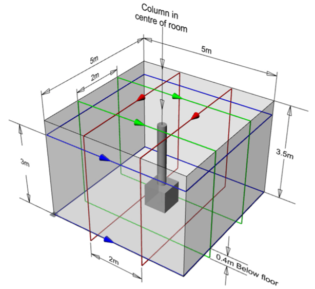
Figure 1. Image Credit: Spicer Consulting Limited
It is advisable to draw the cables below the floor when working with TEMs fitted with a Gatan Imaging Filter (GIF), because the GIF is located underneath the microscope column and, therefore, requires canceling at a lower height.
SEMs with small columns may not require a large, canceled volume, meaning that a minimal cable layout may be sufficient.
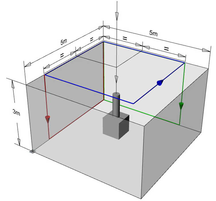
Figure 2. Image Credit: Spicer Consulting Limited
In these circumstances, cables may be drawn in three loops to form three planes that do not intersect the microscope (Figure 2). This solution is cost-effective and straightforward, requiring no cables to be placed on the floor and no major alterations to the room.
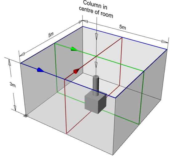
Figure 3. Image Credit: Spicer Consulting Limited
Where there is a requirement for improved performance, the X and Y cables should cross the room above the microscope column (Figure 3). This is because drawing the loops closer will enhance the canceling ability of the system.
Summary
It is important to cancel out external magnetic fields to enhance the performance of electron microscopes, which can be achieved using the SC24 Magnetic Field Cancelling System.
By utilizing two sensors positioned on either side of the column and taking the average of their measurements, it is possible to measure the field at the point of interest.
Once this is known, an array of cable set-ups can be employed to accommodate the specific system and infrastructure requirements.

This information has been sourced, reviewed and adapted from materials provided by Spicer Consulting Limited.
For more information on this source, please visit Spicer Consulting Limited.