Semiconductor components have gained universal prominence, playing an essential role in everyday life. They influence global communication, shape interactions, offer amusement, and enable various modern conveniences.
With the proliferation of interconnected products and services, safeguarding their consistent availability has become a strategic imperative while the exigencies of advancement persistently shift.
To address these mounting demands, manufacturers of these components have embarked on a trajectory of pushing scaling limits and ushering in novel materials and processes, necessitating inventive advancements in the realm of critical semiconductor equipment.
Semiconductor manufacturing is generally divided into two sections; “front-end,” which is focused on wafer fabrication, and “back-end,” which involves the assembly of an integrated circuit.
These processes require very high precision, which also translates to the equipment used.
This article will highlight the differences between the two sections, as well as some of the sealing solutions required for back-end semiconductor processing and their benefits. Many of today’s demanding applications require processes in which the equipment capabilities are optimized to provide the highest possible yields at the lowest possible cost.
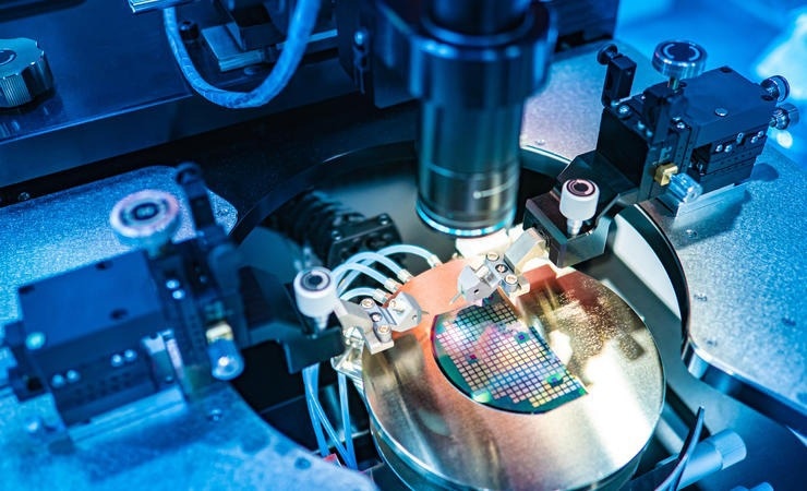
Image Credit: Omniseal Solutions
Brief Overview of Front-End Semiconductor Manufacturing
In a previous article, Omniseal delved into front-end semiconductor manufacturing and the advantages of polymer solutions. The front-end procedure necessitates a multitude of intricate phases to convert a wafer into a completed device.
These steps include wafer cleaning, oxidation, and photolithography to pattern devices as well as a series of etching, deposition, doping, and metallization steps.
Furthermore, inspection and metrology equipment is used for process control. This is when the wafers are inspected to identify irregularities that have the potential to induce issues with for the end-product.
Optical techniques are used, and e-beam inspection is often required to find the smallest defects. Throughout this manufacturing process, Omniseal Solutions’ high-performance seals are employed and deliver exceptional performance under demanding conditions such as elevated temperatures, aggressive chemical and plasma environments, and ultra-high vacuum circumstances.
These seals find application in a wide array of equipment, including chemical vapor deposition (CVD) and plasma etching systems. Alongside the front-end procedure, these solutions also extend to the back-end process.
Key Processes in Back-End Semiconductor Manufacturing
Wafer Probe
In this phase of the semiconductor manufacturing process, the team examines whether the devices conform to the design specifications. While still on the wafer, microcontacts engage with the circuits for testing. Probes then assess and interpret signal responses, with those that exhibit failures undergoing repair or being discarded.
Wafer Dicing
Wafer dicing involves slicing the semiconductor into separate dies. Traditionally, saw dicing was the method employed. However, recent years have seen a notable shift towards slimmer and smaller semiconductor chips, prompting the development of innovative techniques like laser dicing.
Die Bond
The individual dies are too intricate and fragile to be handled on their own. As such, they must be safeguarded. Die Bond is the process of securing the die to the substrate. The substrate then serves as the interface between the chip’s microscopic scale and the electronics manufacturing macroscopic scale.
Wire Bonding
The subsequent step involves wire bonding, which connects each pad on the die to a corresponding one on the substrate via a wire, thus establishing an electrical link. Alternatives like flip-chip techniques can also be applied.
Encapsulation
The bonded die and frame must be sealed to complete back-end semiconductor processing. This can be done using a molded plastic compound or by attaching a sealed lid. At this point, the semiconductor part is ready to be used in electronics manufacturing. Final testing can be done before shipping the completed chip.
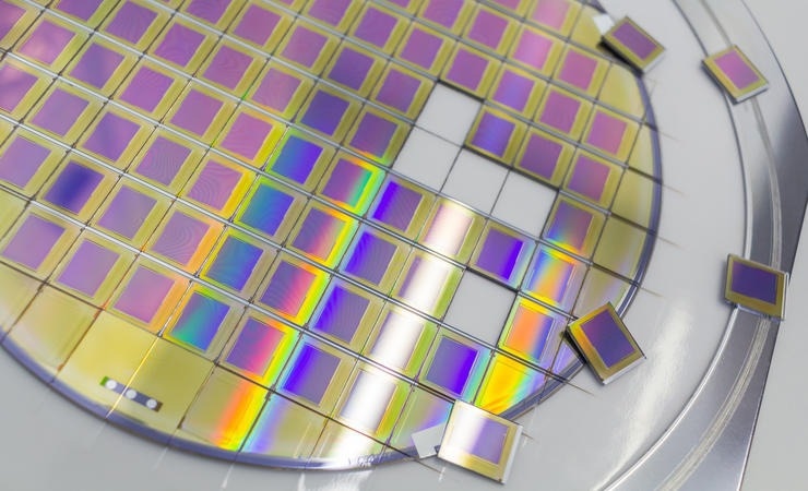
Image Credit: Omniseal Solutions
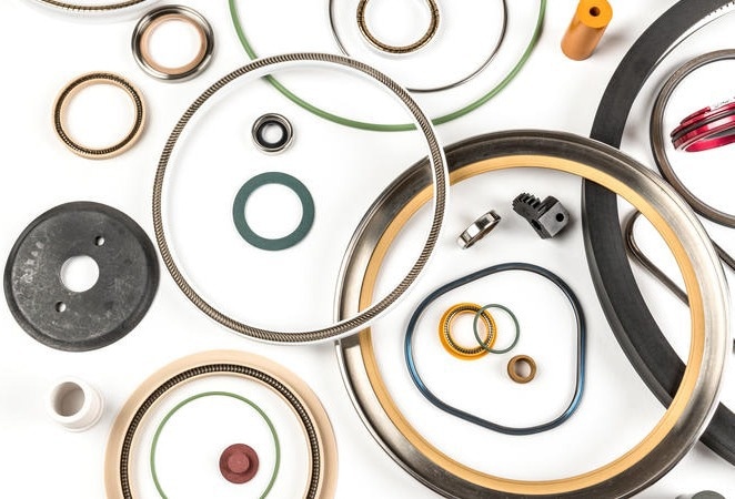
Image Credit: Omniseal Solutions
Semiconductor Sealing & Material Solutions from Omniseal Solutions
Omniseal Solutions engineers and manufactures high-performance wear and sealing solutions that are part of the back-end semiconductor manufacturing processes outlined above, which include a broad range of precision equipment such as SMT Dispensing and Pick & Place Test Handlers.
These solutions help to address challenges in the assembly and test processes of back-end manufacturing.
As a global enterprise, Omniseal Solutions exhibits agility in delivering tailored solutions spanning the complete semiconductor value chain. Among its services is expedited prototyping, where the design team generates a prototype and delivers a solution engineered to the strictest of tolerances.
Omniseal® spring-energized seals and metal face seals are top-tier sealing choices designed to address pivotal prerequisites in the equipment sector. This encompasses enduring extreme temperatures and pressures and withstanding corrosive chemicals and other hostile media.
Omniseal Solutions also offers custom machined components, including its Meldin® polyimide solutions designed for bearings, CMP retaining rings, clamp rings, and bespoke components.
Other benefits include:
- Low wear and friction
- High purity and low outgassing
- Electrical insulation
- Reduction in maintenance and downtime

This information has been sourced, reviewed and adapted from materials provided by Omniseal Solutions.
For more information on this source, please visit Omniseal Solutions.