The VOYAGER is a high-performance electron beam lithography system that has been specifically developed and is appropriate wherever direct access to electron beam lithography in multi-user facilities is needed.
The entirely automated and ultra-ergonomic system together with smart features and original system architecture guaruntees the shortest time to result. This makes it perfect for both academic and industrial surroundings.
With features including:
- Stitching-error-free continuous writing modes traxx and periodixx, based on moving stage technology
- 50 kV thermal field emission column technology
- Highly ergonomic human-machine interface ErgoFlow
- Unique formula-based patterning technology algorithmixx
- Flexible directional shape-filling modes FLEXposure
- Automatic focus and stigmator setup
- Automatic switch between high-resolution and high-throughput writing modes
- Fully automated write field calibration
VOYAGER stands for user-friendliness, innovation and stable high performance all at an affordable price/performance ratio throughout the lifetime of the instrument. The VOYAGER electron beam lithography system comes with an environment-tolerant shield that ensures system stability even in less-perfect laboratory surroundings.
EBL at the push of a button
Video Credit: Raith
Ergonomic Interface and Automated EBL for Shortest Time to Result
VOYAGER makes use of Raith’s eWrite technology. eWrite integrates faithful EBL electron optics along with the new innovations in pattern generator design that makes automated system calibrations and batch fabrication possible.
All corrections that are required throughout the complete exposure job are applied pixel by pixel and “on the fly.” This helps save huge process time overheads. Depending on the pattern, writing speeds of more than 1 cm²/hour could be obtained at the highest resolution.
Furthermore, the degree of automation goes one step further thanks to the new ergonomic human–machine interface known as ErgoFlow. Making use of this smart workflow, professional lithography becomes more accessible to everyone—no matter their level of expertise.
ErgoFlow complements the widely used Raith Nanosuite standard software and comprises two elements.
In the initial step, it is possible for any user to easily specify an EBL job. This has to be additionally parameterized and executed in the second step by a experienced user. With the help of VOYAGER’s unique sample leveling system, even manual leveling, and pre-alignment are automatically regulated. This helps save time and considerably increases efficiency.
ErgoFlow is easy to use and could also leverage interdisciplinary research and sample exchange even between diverse university faculties or industrial departments.
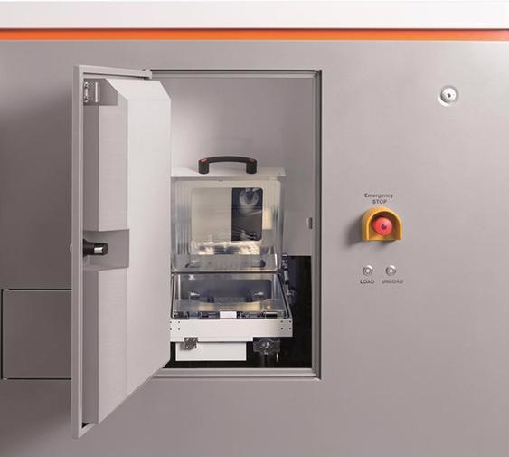
With its innovative architecture VOYAGER allows for a cost-effective “through-the-wall-loading” setup of the e-beam writer. Image Credit: Raith GmbH
Features
Stitching and Overlay
≤ 20 nm
Beam Current Stability
≤ +/− 0.2%/hour
Guaranteed Minimum Linewidth
≤ 8 nm
A High-Performance Electron Beam Lithography System with Innovative Architecture and Unique Application Solutions
Both software and hardware have been developed for automated exposure operations. Special software features like the new formula-based patterning technology algorithmixx and the constant-moving-stage-based writing modes traxx and periodixx help users increase their efficiency and perfect device performance.
Applications utilized in the fields of photonics, optics, and optoelectronics benefit from the software solutions that are available. It is possible to
- Tune grating pitch in the 10 pm regime
- Regulate extremely large design data sets in an efficient manner
- Losses can be decreased in tapered waveguides
Applications
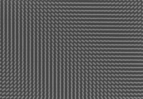
Metalens structure using efficient formula based patterning. Image Credit: Raith
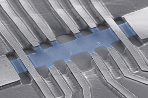
150 nm gate in PMMA (bi-layer). Image Credit: Raith
Freestanding multi-terminal graphene device. Image Creadit: M. Kühne, MPI Stuttgart, Germany.
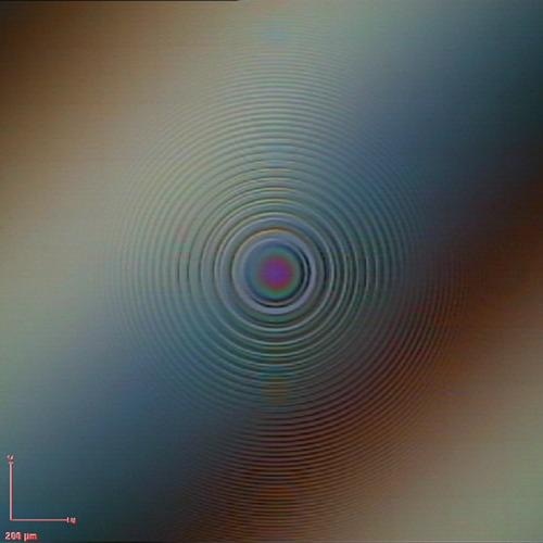
Center of a 1x1 cm² fresnel lense in SU-8 written in 53 minutes. Image Credit: Raith
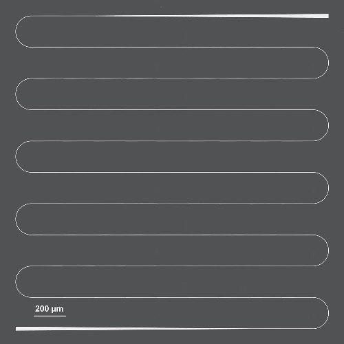
Stitching-error-free high-performance tapered waveguides, several mm in length. Image Credit: Raith
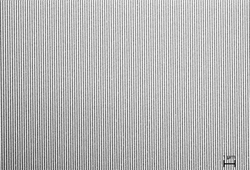
1x1 cm² grating in ZEP520a in less than 2 hours. Image Credit: Raith
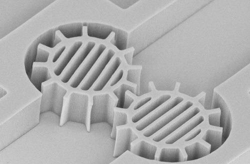
Micro gear pump. Image Credit: Raith
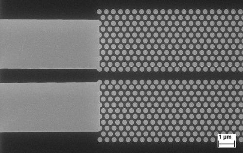
Photonic crystal waveguide in ZEP520a. Image Credit: Thomas Krauss, University of York, UK
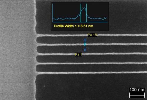
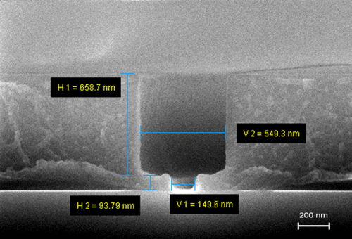
Sub-7 nm lines in HSQ. Image Credit: Raith
Service
Clear drivers of decision-making are system performance and specifications parameters where EBL systems are considered. However, there is a need for several factors to be taken into account if efficient operation, reliable support, and continuous uptime are to be ensured over the lifetime of the instrument system.
Using a global team of professional service engineers, Raith Service ensures users can make the ideal use of their system. When users decide on a Raith system, all site surveys jointly with surrounding measurements, the resultant factory, cleanroom laboratory setup, and on-site training are involved.
Moreover, application aids are available free of charge in all worldwide time zones.
Raith service contracts track a modular scheme and could be configured to match users’ separate budgets and needs.

Image Credit: Raith