The most productive EBSD technology available for examination of the microstructure of metals; the Thermo Scientific™ Quasor™ Electron Backscatter Diffraction (EBSD) system offers a highly efficient CMOS sensor designed to provide highly efficient characterization in the SEM.
This instrument is designed with the primary goal of increasing productivity; offering fast rates of collection and accurate indexing of electron backscatter diffraction patterns. The Quasor™ EBSD can operate under low light conditions and comes integrated with the Thermo Scientific™ Pathfinder™ X-ray microanalysis software. This acclaimed software is capable of simultaneously analyzing the microstructure of a material as well as its elemental chemistry, so that meaningful results can be acquired quickly and easily.
Quasor’s revolutionary CMOS camera offers metallurgists the ideal tool to improve throughput rates in their SEM lab, while gaining a more in-depth understanding of the materials they are studying.
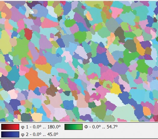
Euler map obtained from low carbon steel composed of ferrite grains. This data was collected with a 1 millisecond per pixel dwell time.
Making EBSD a Reality
- A signal-to-noise ratio that is three times better than other CMOS cameras
- Up to 600 frames per second collection rates, with over 99 % of pixels indexed
- A single measurement provides chemical and structural information
- Integrated Pathfinder™ software, offering X-ray microanalysis for simultaneous collection of EDS/WDS and EBSD data
Designed for Metallurgy
- SEM-based methods can be developed for quality control and failure analysis.
- Phase identification and transformation analysis can be performed after heating and cooling.
- Phases and size grains can be easily identified.
- Heat affected zones can be monitored following welding.
- Predictive heat fracture analysis of metals can be carried out.
- Additive manufacturing processes can be validated with ease.