EV Group (EVG), a leading supplier of wafer bonding and lithography equipment for the MEMS, nanotechnology and semiconductor markets, today announced that the Singapore-MIT Alliance for Research Technology (SMART) has ordered an EVG®850LT fully automated production bonding system designed for silicon-on-insulator (SOI) and direct wafer bonding using low-temp plasma activation processing.
SMART, which is a leading research center established by the Massachusetts Institute of Technology (MIT) in partnership with the National Research Foundation of Singapore, will utilize the EVG850LT system to support its advanced substrate development efforts.
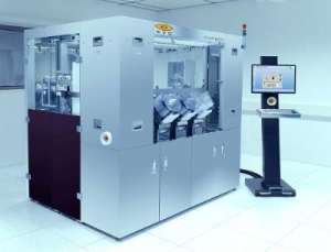 The EVG(r)850LT fully automated production bonding system combines all essential steps for wafer bonding in a single platform to ensure an ultra-clean production process throughout all stages, thereby enabling high-yield, void-free wafers. It supports a variety of advanced substrates, including silicon-on-insulator (SOI) and silicon on lattice engineered substrate (SOLES) technology, up to 300 mm in diameter. (PRNewsFoto/EV Group)
The MIT research center is located outside the United States in Singapore and has five different research groups, including the Low Energy Electronic Systems (LEES) Research Group, which focuses on integrating silicon CMOS and compound semiconductor materials to enable new integrated circuits (ICs) for wireless devices, power electronics, LEDs, displays and other applications. The LEES Research Group features a state-of-the-art fabrication facility, where the EVG850LT has already been installed and is in use.
According to Professor Eugene Fitzgerald from MIT's Department of Materials Science and Engineering, SMART chose the EVG850LT for the center's advanced R&D efforts due to the system's high process flexibility and performance, EVG's experience in low-temperature bonding, and expertise and support in process development. "The charter of our LEES Research Group is to identify new IC technologies that enable devices that consume less power, enable higher performance and open up new applications for information systems. EV Group's technology and expertise will play an important role in supporting this effort," stated Professor Fitzgerald.
The EVG850 platform, upon which the EVG850LT system is built, is the only SOI and direct wafer bonding platform designed to operate in high-throughput, high-yield environments—establishing it as the industry standard in the SOI wafer bonding market. The EVG850LT platform combines all essential steps for wafer bonding—from cleaning and alignment to pre-bonding and IR-inspection—in a single platform. This ensures an ultra-clean production process throughout all stages to enable high-yield, void-free wafers, as opposed to stand-alone processing units that require the wafers to be manually transported in a regular cleanroom environment. The EVG850 supports a variety of advanced substrates, including SOI and silicon on lattice engineered substrate (SOLES) technology, up to 300 mm in diameter.
"EVG has been at the forefront of SOI technology development for more than 20 years, and has established a strong expertise and leadership in engineered substrate bonding. We have worked closely with leading research institutes and inventors of SOI technology, and we are very proud that SMART has chosen our high-throughput, high-yield EVG850 system for their advanced technology development efforts," said Frank Huysmans, regional sales director, Asia/Pacific at EV Group. "This is a testament to our leadership in engineered substrates, from R&D to high-volume manufacturing. SOI wafer producers and researchers rely on EVG's equipment to advance the production and technological capabilities of SOI wafers."
About EV Group (EVG)
EV Group (EVG) is a leading supplier of equipment and process solutions for the manufacture of semiconductors, microelectromechanical systems (MEMS), compound semiconductors, power devices and nanotechnology devices. Key products include wafer bonding, thin-wafer processing, lithography/nanoimprint lithography (NIL) and metrology equipment, as well as photoresist coaters, cleaners and inspection systems. Founded in 1980, EV Group services and supports an elaborate network of global customers and partners all over the world.