EV Group (EVG), a leading supplier of wafer bonding and lithography equipment for the MEMS, nanotechnology and semiconductor markets, today announced that it has received multiple orders for its GEMINI® FB XT automated fusion wafer bonders from multiple leading device manufacturers.
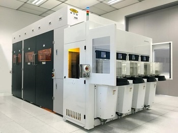 GEMINI® FB XT automated production fusion bonding system
The GEMINI FB XT offers industry leading wafer-to-wafer alignment accuracy, customizable pre- and post-processing configurations with faster handling and improved process flows that increase throughput by up to 50 percent compared to the previous-generation platform, as well as integrated metrology to maximize yields and productivity in high-volume manufacturing (HVM). These latest orders for the GEMINI FB XT system will support several leading-edge HVM applications, including 3D stacked image sensors, memory stacking, and die partitioning for next-generation 3D system-on-chip (SoC) devices.
Vertical stacking of devices has become an increasingly viable approach to driving continuous improvements in device density and performance without the need for increasingly costly and complex lithography processing. Wafer-to-wafer bonding is an essential process step to enable 3D stacked devices. However, tight alignment and overlay accuracy between the wafers is required to achieve good electrical contact between the interconnected devices on the bonded wafers, as well as to minimize the interconnect area at the bond interface so that more space can be made available on the wafer for producing devices.
These latest orders for our GEMINI FB XT system from multiple leading manufacturers reflect the fact that our most advanced fusion bonding platform meets critical production requirements for a variety of 3D chip stacking applications, and further demonstrates our leadership in fusion bonding. Unparalleled wafer-to-wafer alignment accuracy supports IC manufacturers' efforts to move wafer stacking upstream from back-end-of-line (BEOL) and mid-end-of-line (MEOL) applications to front-end-of-line (FEOL) processing where they can integrate more functionality into their product at the wafer level and further drive down manufacturing costs. The GEMINI FB XT has proven to fulfill the most stringent compatibility requirements and standards of state-of-the-art front-end fabs. It also combines the capabilities necessary to bring new bonding technologies, like hybrid bonding for CMOS image sensors, into high-volume production. It is a true testament to our Triple-i philosophy of invent, innovate and implement.
Hermann Waltl, executive sales and customer support director at EV Group
Leveraging EVG's XT Frame platform and an equipment front-end module (EFEM), the GEMINI FB XT automated production fusion bonding system is optimized for ultra-high throughput and productivity. It incorporates EVG's proprietary SmartView® NT face-to-face aligner to achieve wafer-to-wafer overlay alignment accuracy below 200 nm (3 sigma), which leads the industry in performance and is essential to enabling 3D integration. In addition, the system can accommodate up to six pre-and post-processing modules for surface preparation, conditioning and metrology steps--such as wafer cleaning, plasma activation, alignment verification, debonding (allowing pre-bonded wafers to be separated automatically and re-processed if necessary) and thermo-compression bonding. This enables the GEMINI FB XT to support fully automated and integrated wafer loading, alignment, bonding and unloading of bonded wafers in HVM environments
25 Years of Technology Leadership in Wafer Bonding
For nearly 25 years, EVG has revolutionized automated wafer bonding, and today is the technology and market leader with the largest installed base of automated production wafer bonding systems worldwide. The company launched the first automated wafer bonding systems in 1992, patented its SmartView wafer-to-wafer alignment system in 1999, and introduced its LowTemp™ plasma bonding technology in 2003. The first GEMINI FB fusion bonding system with optical alignment for back-side illuminated image sensor and 3D-IC manufacturing was installed at leading HVM customers' fabs in 2009. With the latest product generation--the GEMINI FB XT automated production fusion bonding system--EV Group has successfully implemented fusion and hybrid bonding for producing today's most innovative 3D CMOS image sensors, stacked DRAM and memory-on-logic devices.