During the manufacture of semiconductor wafers, thickness measurement forms an important part of this process, since it provides process engineers with the information required to ensure that manufacturing processes are under control and rates of material removal are within the specifications of customers.
To this end, thickness measurement devices must be able to produce precise and accurate readings without contacting the surface of wafer. For non-contact measurement of electrically conductive materials, capacitance based measurement probes are generally used.
Capacitance-based Thickness Gages
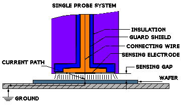
Figure 1. Single probe system
Capacitance-based thickness gages employ insulated sensing electrodes, which are capable of detecting changes in distance between the target surface and the probe face (Figure 1). This distance, also known as the sensing gap, is directly proportional to a change in capacitance.
From the probe face, electrical current flows via the target and sensing gap. The circuit is completed when the target finally lays on an electrically grounded stage. Thickness can then be measured by comparing the variation in capacitance between a known sensing gap, and the gap when an object with unknown thickness is positioned under the probe face,
However, capacitance measurements of electrically grounded targets are compromised by variations in the electrical conductivity of the target being measured.
When measuring wafers of differing resistivities, the accuracy of the device is affected when the electrical ground path from the target to the sensing probe becomes irregular and vague.
Thickness Measurement Device
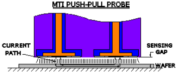
Figure 2. Push-Pull probe
In order to prevent the effect of varying target conductivity, MTI Instruments has designed a thickness measurement device that uses a special version of its Accumeasure probe/amplifier series, known as the Push-Pull (MTI-1560).
The push-pull probe (Figure 2) prevents the necessity for a consistent ground between the stage and the wafer. The probes are calibrated to create an AC voltage signal of equal amplitude from 0 to 5VAC.
However, there is a 180 degree phase shift between the signals that enables the current path to pass across the target surface instead of via the target to ground. The amplifier sums up individual output signals, creating a 0 to 10VDC output.
System Design
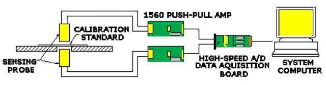
Figure 3. Wafer measurement gage schematic
During the processing of semiconductor wafers, bow and warp are introduced to the wafer profile. Hence, to obtain a true thickness measurement a probe can be placed on either side of the wafer to prevent these surface irregularities from affecting the thickness calculation. A basic schematic of the measurement system is shown in Figure 3.
When a wafer is positioned between the probes, analog voltage outputs are made to pass from the 1560 amplifiers to a high speed PC-104 A/D data acquisition board. Following this, the CPU transforms the voltage to a gap distance by means of a calibration table. The thickness of the wafer is measured and displayed on the LCD.
Modes of Operation
While taking thickness measurements of semiconductor wafers, the software includes two modes of operation: 5-point measurement and continuous read modes. In 5-point measurement mode, the user shifts the wafer such that an optimum point on the surface is between the probes, and starts a reading by punching a key on the user interface. The measurement from each point is stored and sent to a PC or printer through the on-board RS-232 port.
In continuous read mode, voltage outputs are continually transferred to the CPU through a data acquisition card. The CPU then calculates an average thickness based on 50 data points and shows the result on the LCD.
Before assembling the measurement system, the amplifiers circuits are calibrated by means of a Mitutoyo Calibration Stand (Model 521-104), which is able to move the target in increments of 0.00001”.
Results and Discussion
Measuring wafers of varying resistivities has no impact on the accuracy of the device. Also, electrically grounding or un-grounding of the measurement stage had no effect on the accuracy of measurement.
Thickness measurements were obtained utilizing each part of the voltage output range without affecting device accuracy. Furthermore, tests measuring materials with different bulk resistivity have demonstrated that recalibration of probes is not required for variations in target material.
From the above discussion, it is evident that the MTI-1560 amplifier and probes can precisely measure materials with electrically conductive surfaces. One can easily customize the thickness device to accommodate a sensing range of +/- 0.005” and a maximum thickness sensing range of 0.040”.
About MTI Instruments
MTI Instruments is a worldwide leader in the design, manufacture and engineering of non-contact measurement systems and sensors.
MTI’s main products consist of computerized general gauging instruments for position, displacement, thickness and vibration applications based on laser triangulation, fiber-optic and capacitance measurement technologies.
Microtrak Pro 2D Laser Sensor, MTI’s newest product innovation, offers an economical, industrial, high precision solution to your position, displacement and profile applications.

This information has been sourced, reviewed and adapted from materials provided by MTI Instruments Inc.
For more information on this source, please visit MTI Instruments Inc.