Donald K. Cohen, Ph.D., founder of Michigan Metrology, talks to AZoM about the history of optical profiling, it's development and industry applications.
What does Michigan Metrology do and how did it get started?
Since 1994, Michigan Metrology has been providing 3D surface microtexture and wear measurement and analysis services using Bruker 3D optical profilers. I work with all types of industry, from automotive to chemical and materials to medical devices.
A typical project might involve understanding how the surface texture of a component affects its tribological properties, such as friction or lubricant retention. Other projects may be related to measuring the 3D surface characteristics of a wear pattern to help determine the possible wear mechanisms at work.
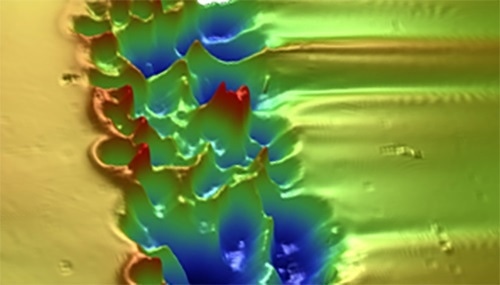
3D optical image showing defect in chrome plating. © Copyright Bruker 2017
I was fortunate to be involved in the early development of 3D optical profiling, before spinning out and starting Michigan Metrology, and I am pleased to see that the measurement technique is being used routinely now, and is even appearing in the literature as simply OP, just like SEM, AUGE, or ESCA.
When did 3D optical profiling get started?
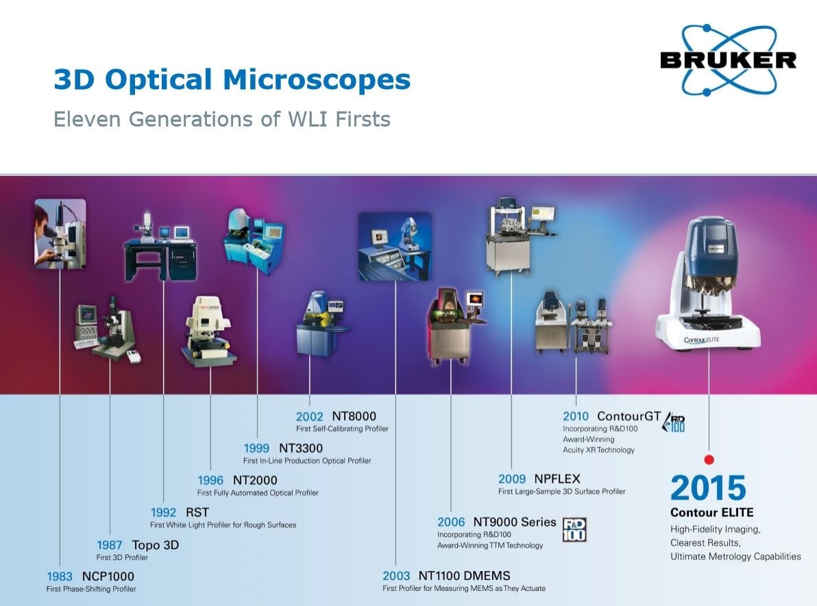
Back in the 1980s, Dr. James C. Wyant from the University of Arizona started WYKO, a company that initially developed some of the first phase shifting interferometric (PSI) profilers, which were used to measure polished optical surfaces. These 2D profiling instruments (the NCP 1000 profilers) were limited to measuring average roughness (Ra) of about 0.05 microns (2 microinches). So at this time, the “application” drove the development of the “instrument.” However, word quickly got out and other industries, in particular the magnetic tape and disk drive industry, began using these profilers for critical surface inspection. Funded and supported by Dr. Bharat Bhushan of IBM, WYKO then developed the world’s first 3D non-contact optical profiler, the TOPO-3D. I was fortunate to join WYKO around the launch of the TOPO-3D, as product manager.
What were some of the early applications for the TOPO-3D
The magnetic disk drive industry was key in driving the growth of the optical profiling technology being used to measure the disk surfaces at various stages of production, as well as the magnetic recording heads. It turns out the mag heads had many characteristics besides surface roughness that needed to be measured with optical profiling, such as slider crown, slider camber, slider flatness and pole tip recession. Suddenly, optical profilers were measuring micro-form as well as texture. The mag storage industry began first using optical profilers as a QC tool, with maybe a few instruments per plant, typically in the off-line QC room. Now, optical profilers are integral to the magnetic disk drive manufacturing process.
What drove further development of optical profilers?
Rougher surfaces was a big driver. As the TOPO-3D was being introduced in the late 1980s, it was becoming clear that there was a need to measure in three dimensions the surface texture of surfaces with Ra greater than 0.05 microns. For example, magnetic tape providers needed to measure the back side of the tapes, which the TOPO-3D was not able to characterize. The mag heads were also being designed with step-like features much greater than 1 micron that needed to be inspected. In addition to the industries that were familiar with TOPO-3D, other scientists and engineers in the automotive, medical device, and printing industries were seeking a solution for measuring their surfaces in 3D.
How was this need to measure rougher surfaces addressed?
Around 1990, WYKO developed vertical scanning interferometry (VSI), a technique that allowed the 3D measurement of roughness values of ~3 microns and peak-to-valley heights of ~100 microns. (These roughness values by the way, are now called Sa rather than Ra to reflect that the measurement is over an area rather than a profile ). The company developed a new profiler to take advantage of the VSI mode, the WYKO RST (for rough surface tester). With both the VSI mode and PSI mode, measurements were limited to an area of about 1 millimeter x 1 millimeter, although new interferometric lenses were introduced quickly that allowed both higher magnifications (measurement areas of about 200 microns x 200 microns) and lower magnifications (measurement areas of about 3 millimeters x 3 millimeters). Early applications included measuring printing plate ink capacity used for magazines and shot-peened gear surfaces used in the automotive industry for fatigue strength enhancement.
Once the WYKO RST was developed, the technology began driving the applications, which was a very interesting shift. At this point, many industries previously unfamiliar with 3D optical profiling were being made aware of the technique. The advances in the technology were giving manufacturers an edge over their competition. Even today I run into applications where people are unware of the technique and see measurements in my lab for the first time, opening up new and deeper levels of understanding for their applications. This increased understanding directly translates into more advanced designs and better product performance.
What are some of the current applications for 3D optical profiling?
Many types of applications have emerged for development and inspection needs over a wide variety of industries with radically different measurement requirements, such as the optical fiber industry versus the medical device industry. For example, real-time optical profiler measurements are needed to investigate the moving structures in the scanner chips used in DLP projectors. In automotive plants around the world, 3D optical profilometry is being used to measure items such as the grind pattern on engine valves, the texture inside engine cylinders, and the critical characteristics of fuel injectors. In the consumer products arena, items such as plumbing products (e.g., faucets), the nature of the packaging materials used for foods (e.g., potato chips), and even the texture of the components used to deliver deodorant are all making use of 3D optical profiling for product development and manufacturing inspection.
What further instrument developments have occurred to improve the reach of the technique?
Back in the mid 1990s, with the advancing power of the PC, optical profilers began to be able to stitch together multiple high-resolution images to measure larger image areas without sacrificing lateral resolution. In the early days, maybe 10 or so images could be stitched. Today it is possible to stitch hundreds of images to produce striking measurements of very rough surfaces. Other technologies, such as measuring the characteristics of semi-transparant films, advanced automation or image processing, and large sample configurations have been achieved.
What does the future look like for the 3D optical profiler?
Applications are continuing to develop, which will further drive the technology, particularly in the areas of throughput as 3D optical profiling continues to move from a QC inspection instrument to an in-line process control tool. Additionally, the cost of the instruments continues to drop, making 3D optical profiling as common as any other microscopy technique in a typical materials lab. All of the advances that go into making a car more fuel efficient, or a smart phone smarter will at some level be the result of or the driver for new optical profiling capabilities and techniques. I can tell you from first hand experience, the measurement game is never boring, and I can’t see that changing anytime soon.
About Donald K. Cohen

In 1994, Dr. Cohen established Michigan Metrology to help engineers and scientist solve problems related to “leaks, squeaks, friction, wear, appearance, adhesion, and other issues,” using 3D Surface MicroTexture Measurement and Analysis.
Dr. Cohen has been Chairman of the STLE-Detroit section and has been active with the ASME B46.1 committee on surface texture since 1988, having served as Chair from 2005-2011.
Dr. Cohen has an undergraduate degree in Physics from the University of Michigan – Dearborn and graduate degrees in Physics and Optical Sciences from the University of Arizona.
Early in his career, Dr. Cohen worked with IBM on optical disk drive development. He later joined WYKO Corporation as Product Manger and finally Vice President, developing 3D surface texture metrology instrumentation.
Disclaimer: The views expressed here are those of the interviewee and do not necessarily represent the views of AZoM.com Limited (T/A) AZoNetwork, the owner and operator of this website. This disclaimer forms part of the Terms and Conditions of use of this website.