Surface metrology has to increasingly deal with the presence of sub-micron thick films, which are now being used on products well beyond semiconductor devices. Sub-micron films may be incidental – for instance, oil on a machined part – or may not be very important to users who are interested only in the top surface. However, the film may also be vital, providing specific optical characteristics or protecting the underlying substrate.
In any situation, introducing a sub-micron film to a component seldom relaxes prior surface metrology requirements. Such requirements will often expand to include film properties such as texture, thickness, and uniformity.
Requirements for Surface Films Analysis
Preferably, a surface metrology technology developed to determine sub-micron films will be able to retain its performance only for topography. This includes metrics such as throughput and resolution and even extends to configuration flexibility. In the case of microscope-based technologies, this would mean that surface films analysis should not limit the choice of zoom or objective.
As for the films metrology itself, it is imperative that associated calibrations are sample-agnostic – a calibration artefact that is specific to a sample, for instance a matching bare substrate may be either impractical or costly. It is best if measurements leverage the available optical resolution: surface metrology that was earlier generating high-resolution height maps should do similarly for thickness. Ultimately, surface films analysis should be able to give definite results across a broad thickness search range. Users may not know much about thickness, or thickness may differ widely over the measurement area.
The Challenge and Opportunity for Coherence-Scanning Interferometry
Coherence scanning interferometry (CSI) is capable of providing non-contact areal topography maps with sub-nm precision [1][2] across a wide range of surface types, such as flat panel display components [3][4], automotive machined metal parts [5], patterned semiconductor wafers, MEMS devices, and transparent film structures. CSI measures surface topography from the localized coherence signal generated by interference between reflections from a reference surface and the sample. A standard CSI signal for a bare surface (that is no film) is depicted in Figure 1(a): surface location basically corresponds to the peak envelope position.
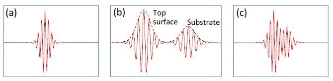
Figure 1. Typical CSI signals for (a) bare surface (no film); (b) thick film (well over 1 µm) with well separated signals from surface and substrate; and (c) sub-micron film with merged surface and substrate signals.
In general, a transparent film will create an extra signal from the substrate. In the case of thick films (Figure 1(b)), the signals are suitably separated and can be conveniently assigned to the substrate and top surface [6][7]. Conversely, for sub-micron films the substrate and surface signals combine together (Figure 1(c)) and cannot be separated. This sensitivity to films also presents a new possibility: the distorted CSI signal can be decoded by modeling the film effects, enabling simultaneous measurement of thickness and surface.
Model-Based Csi
Previous Approaches
In this context, model-based CSI replicates signals over a predicted range of film properties and chooses the best possible match with the measured signal. It has been demonstrated in different forms [8][9][10][11][12], all using frequency-domain analysis to integrate models for the system and of the part being determined.
There is a caveat with model-based CSI: it is important that film properties are at least partially known, to bind the search space and prevent degenerate solutions. In fact, this often needs to be known for visible-spectrum refractive indices for film as well as substrate, with the thickness of the film left as the unknown parameter to be evaluated.
In previous model-based approaches, there were practical trade-offs between field of view and throughput because of intensive computation, and often precluded the use of high-NA objectives. Thanks to the precursor to the method described here, high-NA measurement of samples with complex reflectivity is achieved [13][14][15], by means of a system model derived from the objective pupil to create signal libraries across the wide search range (Figure 2). A specialized Bertrand tube-lens is required to perform the pupil calibration.
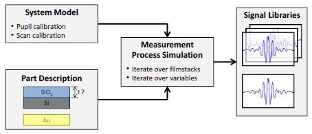
Figure 2. Signal library generation, combining a system model handling arbitrarily high NA with a model of the part being measured.
Presented Approach
While the method illustrated here is similar in principle to its predecessor [13], it divides calibration into two parts: an on-tool component and a nominal pupil calibration carried out with the preferred measurement configuration. The procedure employs only standard CSI hardware and can be applied with any interferometric objective. Figure 3 shows the entire measurement sequence.
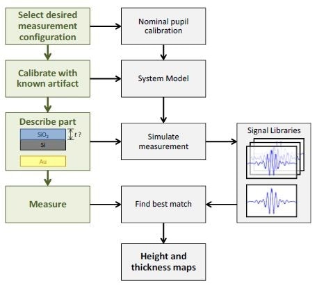
Figure 3. Measurement flow for presented approach. Steps performed by the user are shown in green.
The best-match signal search remains technically unchanged, with the main difference that optimized processing –enabled by greater computing power – now facilitates full-field analysis at megapixel camera formats. While processing time mostly relies on the pixel count and search range, it is usually under 10 seconds for full-field analysis. Any flat artifact with known visible-spectrum refractive indices are used for calibration. There is a need for no part-specific calibration, which is mostly advantageous for parts with complex geometries or reverse engineering.
Example Measurements
Different types of parts with sub-micron films and dissimilar materials were measured using a contemporary commercial CSI microscope [16]. For each measurement configuration, a silicon carbide flat was used to perform calibration. This silicon carbide flat is also employed for standard-CSI calibrations.
Films Applications Requiring a Wide Search Range
All model-based methods possess some degree of degeneracy that can yield multiple solutions to the same set of model parameters. With regard to films metrology, the result can be incorrect or ambiguous film thickness values that produce apparently acceptable matching signals to the experimental data. Limiting the thickness search range can provide a solution, but this may be precluded by inadequate knowledge or by huge differences in thickness over the measurement area. A more attractive option is to detect small yet clear signal details that make it possible to remove potential degenerate solutions and allow for a wide search range.
A silicon substrate coated with silicon oxide with center thickness ~1.2 µm is illustrated in Figure 4. The coating’s outer rim has a thickness gradient down to zero (bare silicon), where the fixture masks the substrate during evaporation. A 20X Mirau objective was used to measure this transition region, using an oxide-on-silicon model with a search range of 0 to 1300 nm, and separate processing for all pixels in the field of view.
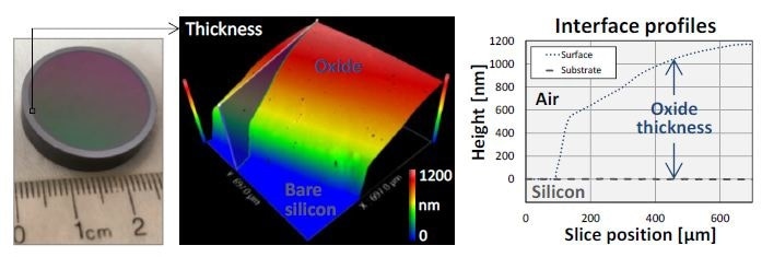
Figure 4. Oxide-gradient sample measured at the film boundary using a 20X Mirau objective. The thickness map ranges from 0 (bare silicon) to ~1.2 µm. The substrate profile, derived by subtracting thickness from the top surface, is flat to ~1 nm.
Figure 4 also shows the resulting thickness map and a cross-sectional slice covering the entire thickness range. As expected, the difference in thickness is monotonic and continuous and indicates that the thickness was explicitly determined throughout the wide search range. As expected, the silicon substrate derived by subtracting thickness from the top surface is flat and within ~1 nm.
Films Metrology over a Wide Range of Magnification
The large choice of magnifications of CSI allow for enables a broad range of surface metrology applications, right from measuring form to investigating microscopic defects. This flexibility, with the addition of thin films, remains just as desirable, and hence should extend to film’s metrology itself. Model-based CSI should ideally work across the entire selection of optical configurations.
Thickness maps, shown in Figure 5, are determined for an oxide-on-silicon film standard (NIST certified thickness of 96.6 ± 0.4 nm) using four different combinations of zoom/objective covering a 70X range in magnification.
For all cases, analysis employed an oxide-on-silicon model with a search range of 0 to 1200 nm for all pixels in the field of view. The wide search range is intentional so as to validate robustness as well as mimic the case of film thickness being unknown.
A complete picture of film characteristics is provided by the wide range of magnifications. The 1.4X Zygo Wide Field (ZWF) objective [19] is able to capture the whole certified region in a single field of view and reveals slow variations in film thickness. In addition, the concentric rings correspond to deliberate patterning in the film, and black rings indicate where the oxide is etched down to the silicon substrate. Measurements performed at higher magnifications show smaller-scale thickness differences and even surface scratches that result from handling this laboratory sample. Details of individual striation defect were revealed by the highest-magnification map, which, in turn, was achieved with a 50X Mirau.
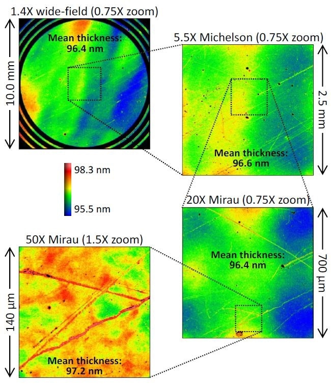
Figure 5. Thickness maps for an oxide-on-silicon film standard (certified thickness 96.6 nm), measured over a 70X range of magnification. The agreement in mean thickness is better than 1 nm across all objectives.
Model-based CSI offers surface maps, in combination with the thickness maps (Figure 4). Subtracting the thickness of film from the top surface creates a derived map of the substrate surface. Together, these maps allow for additional metrology and validation. Yet again, the range of magnifications allows for complete surface analysis.
Results obtained from the 1.4X ZWF capture the regions of the exposed silicon substrate as well as the oxide film (Figure 6). Steps between the oxide and bare silicon are shown by the surface map. From the manufacturing sequence (blanket thermal oxidation followed by patterned etch down to silicon substrate), surface steps are expected to match the thickness of films, or equivalently that the underlying silicon substrate should remain continuous. This is confirmed by the substrate map, validating the overall measurement.
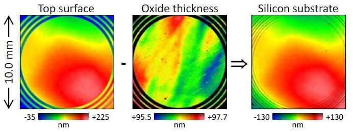
Figure 6. Surface, thickness, and substrate maps for oxide-on-silicon film standard measured using a 1.4X ZWF objective
Measurements performed at higher magnification show textural variations between the surface, substrate, and thickness. Interface maps acquired from the 20X Mirau, with form (4th-order polynomial) removed is shown in Figure 7. The top surface shows both striations and orange-peel texture. In the interim, the film texture is dominated by striations while the substrate shows orange-peel texture but has no striations. These maps together show that the orange-peel texture is contributed by the substrate and the striations reside in the film’s top surface (probably from usage, and not an original defect).
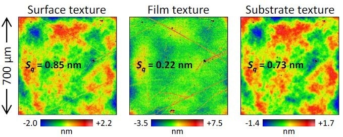
Figure 7. Maps for oxide-on-silicon film standard measured with a 20X Mirau objective, with form removed to reveal texture
Parts with Dissimilar Materials
If there are differences in phase-change on reflection (PCOR), even bulk materials can confound conventional CSI as will take place between different materials [13]. For instance, a traditional CSI measurement of a metal/glass step will be biased by ~10 to 20 nm, with the metal appearing lower than in reality [18].
Traditionally, a part can include both bulk dissimilar materials and films. The fabrication sequence for such a sample is shown in Figure 8, in the form of trenched oxide-on-silicon with a partial gold overcoat.
First, a silicon substrate was used on which about 1 µm of thermal silicon oxide was grown. Then, trenches were formed in the oxide through photoresist masking and a partial etch, and thinner oxide were deliberately left at the bottom of the trench. Lastly, trenches were partly gold-coated by a lift-off sequence (photoresist masking, global gold deposition, photoresist strip). Target gold thickness was approximately 90 nm, which was enough to prevent film effects from the underlying oxide.
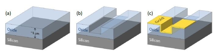
Figure 8. Fabrication sequence for oxide trench sample with partial gold overcoat: (a) grow ~1 µm of thermal oxide on a silicon substrate; (b) form oxide trench; (c) deposit partial gold overcoat.
This sample was determined using a 50X Mirau objective, with analysis customized to each region: an oxide-on-silicon model with a search range of 0 to 1200 nm was used for the uncoated oxide and bulk-gold model (i.e. no film) was used for the gold overcoat. Surface and thickness maps for a pair of trenches over a gold-coating boundary are shown in Figure 9.
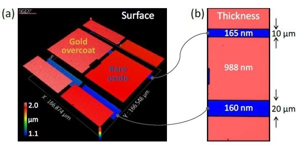
Figure 9. Maps for (a) surface and (b) bare-oxide thickness of trench-oxide sample, measured using a 50X Mirau objective
The thickness of the unetched oxide was determined and found to be 988 nm. For the trenches, thickness slightly relies on their width: 160 nm and 165 nm for the 20-µm trench and 10-µm trench respectively. By subtraction, thickness results indicate a trench depth of 828 nm for the 20-µm trench and 823 nm for the 10-µm trench.
This is confirmed by the results shown in Figure 10, which reveals cross-sectional surface-map profiles via both trenches, and on either sides of the coating boundary, that is, with and without gold overcoat. The trench depths, thus measured, agree with thickness-suggested results to better than 1 nm.
On the whole, thickness and surface results show that the oxide-etch process was approximately 0.6% slower in the narrower 10-µm trench. As further verification, it was observed that trench-depth measurements on both sides of the coating boundary – achieved using independent analyses with and without film effects –agree to better than 1 nm.
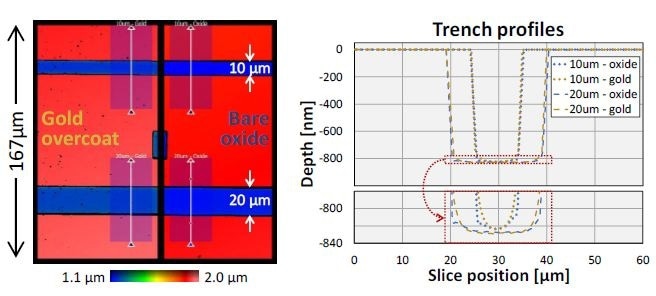
Figure 10. Profiles for trenches with width 10 µm and 20 µm, measured on opposing sides of gold-coating boundary. Measured trench depth agrees to better than 1 nm across the gold-overcoat boundary. The 10-µm trench is ~5 nm shallower than the wider 20-µm trench, consistent with its oxide thickness measuring as 5 nm thicker (Figure 9(b)).
There are certain applications where correct topography is required across dissimilar regions. For this type of sample, this corresponds to the gold thickness step across the coating boundary.
Figure 11 depicts gold-thickness profiles that were determined over dissimilar thicknesses of oxide films: 160 nm inside the 20-µm trench and 988 nm in neighbouring unetched oxide. Both profiles reveal a gold thickness of around 85 nm with agreement to ~1 nm.
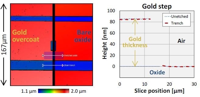
Figure 11. Step profiles across gold-coating boundary, measured within the 20-µm trench and on adjacent unetched oxide. Measured gold thickness agrees to about 1 nm.
Conclusion
This article shows how the presented approach to model-based CSI allows for full-field films surface metrology across an entire range of interferometric objective magnification and yields high-resolution maps of surface and film thickness. Calibration is sample-agnostic, and measurement time for most practical search ranges is similar to that of conventional CSI. Model-based CSI, beyond transparent films, offers PCOR-corrected topography for all combinations of dissimilar materials with known visible-spectrum refractive indices, including metals.
In addition, results show single-nm self-consistency between thickness and topography maps, if refractive indices are well known. This provides a major caveat with model-based CSI: inadequate knowledge of material properties will restrict performance, and can even thwart a meaningful measurement. For model-based CSI, a natural next step would be to extend capabilities to withstand uncertainty in material properties.
Acknowledgments
The original work presented in this paper benefited from key contributions and input from Xavier Colonna de Lega, Jim Kramer and Peter de Groot.
References
[1] de Groot, P., “Principles of interference microscopy for the measurement of surface topography”, Advances in Optics and Photonics 7 (1), 1-65 (2015).
[2] ISO, [25178-604:2013(E): Geometrical product specification (GPS) – Surface texture: Areal – Nominal characteristics of non-contact (coherence scanning interferometric microscopy) instruments] International Organization for Standardization, Geneva (2013).
[3] Grigg, D., Garden, R., Mino, M., Lu, H., and de Groot, P., “New optical metrology techniques for color filter inspection and process control”, Proc. IDW 11th international display workshops, Niigata, Japan (2004).
[4] He, Z., Zheng, J., Garden, R., de Groot, P., “New optical 3D-CD metrology techniques for liquid crystal display manufacture inspection and process control”, Proc. Asia Display, Shanghai, China (2007).
[5] Wyant, J. C., “How to extend interferometry for rough-surface tests”, Laser Focus World, 131-135 (1993).
[6] Flournoy, P. A., McClure, R. W., and Wyntjes, G., “White-light interferometric thickness gauge”, Appl. Opt. 11, 1907 (1972).
[7] Colonna de Lega, X. and de Groot, P., “Transparent film profiling and analysis by interference microscopy”, Proc. SPIE 7064, Interferometry XIV: Applications, 70640I (11 August 2008).
[8] de Groot, P., “Method and apparatus for surface topography measurement by spatial-frequency analysis of interferograms”, US Patent No. 5,398,113 (14 March 1995).
[9] de Groot, P.J. and Colonna de Lega, X. “Signal modeling for low-coherence height-scanning interference microscopy”. Appl. Opt., 43, 4821-4830 (2004).
[10] Kim, S.-W. and Kim, G.-H. “Thickness-profile measurement of transparent thin-film layers by white-light scanning interferometry”, Appl. Opt. 38, 5968 (1999).
[11] D. Mansfield, “The distorted helix: thin film extraction from scanning white light interferometry,” Proc. SPIE 6186, paper 23 (2006).
[12] D. S. Wan, “Measurement of thin films using Fourier amplitude,” US Patent No. 7,612,891 (3 November 2009).
[13] de Groot, P. and Colonna de Lega, X., “Optical Topography Measurement of Patterned Wafers”, AIP ULSI Conference Proceedings 788, 432 (2005).
[14] Colonna de Lega, X., “Generating model signals for interferometry”, US Patent No. 7,619,746 (17 November 2009).
[15] Colonna de Lega, X. and de Groot, P., “Characterization of materials and film stacks for accurate surface topography measurement using a white-light optical profiler”, Proc. SPIE 6995, 69950P (2008).
[16] Zygo Corporation, [Nexview Optical Profiler], Specification sheet SS-0095 09/12 (2013).
[17] Biegen, J. F., “Determination of the phase change on reflection from two-beam interference”, Opt. Lett. 19, 1690-1692 (1994).
[18] Park, M.-C. and Kim, S.-W., “Compensation of phase change on reflection in white-light interferometry for step height measurement”, Opt. Lett. 26, 420-422 (2001).
[19] de Groot, P. and Biegen, J.F., “A new class of wide-field objectives for 3D interference microscopy”, Proc. SPIE 9525, Optical Measurement Systems for Industrial Inspection IX, 95250N (2015).

This information has been sourced, reviewed and adapted from materials provided by Zygo Corporation
For more information on this source, please visit Zygo Corporation