One of the most important aspects of manufacturing of semiconductor devices is consistent and efficient inspection. This can lead to increased yields and thus increased profitability. The product and process must be evaluated after each manufacturing step and feedback provided, particularly during the mass production of wafers (tens of millions of devices per week). It is important to inspect after each stage of the manufacturing process to identify the origin of defects in aspects such as layer thicknesses, step coverage, geometry of critical details, depth of trenches, etc. and subsequently to implement the appropriate corrective measures.
Introduction
The traditional approach to physical failure analysis in semiconductor processing consists largely of perpendicular mechanical polishing or fracture along a defined structure on silicon wafers. Polished sections are usually prepared using a semiautomatic polisher, and the quality of this process is monitored using an optical microscope. Following this step, the polished areas are rinsed in suitable etchants in order to visualize oxide and diffusion layers before they are coated with metal or carbon to allow imaging in an SEM. Fracture of a sample can be carried out either manually or by using dedicated semiautomatic instruments.
Which of these methods is to be used is often determined by the crystallographic orientation of the material as only some are fit for the latter process. There are limitations to these processes, however, as both techniques are time-consuming, the result is largely dependent on the experience of the operator, and regular handling can damage the sample. In addition, there is no possibility for automated navigation to a particular region of interest (ROI) based on data from control systems for either of these two approaches.
Furthermore, the replicability of both methods is relatively low. Cross sectioning using a plasma FIB eliminates these limitations, however, by allowing very accurate site-specific cross-sectioning without the need for extra handling and transfer of the sample back and forth between steps. It also allows navigation to a specific defect on the silicon wafer using data obtained from various manufacturing and inspection systems.
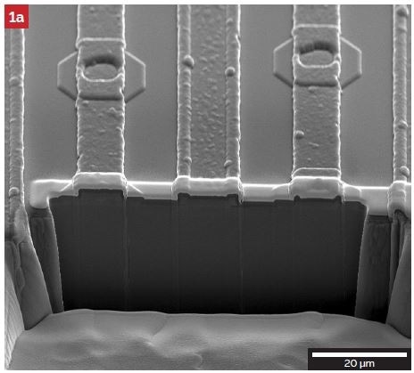
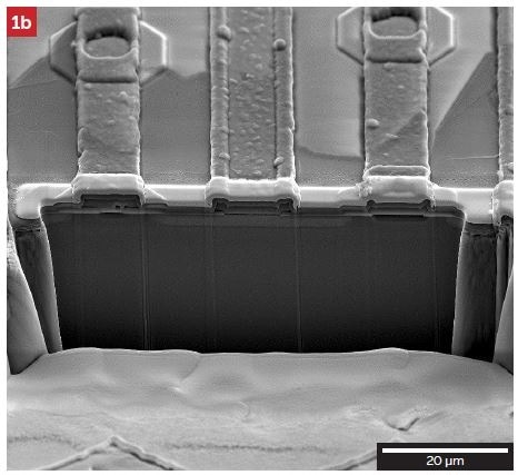
Figure 1. (a) Cross-section before chemical treatment. (b) Cross-section after the etching procedure for the visualization of oxide and diffusion layers.
Results
Sample preparation using the TESCAN FERA3 Xe plasma FIB/SEM involves inserting the whole or part of a wafer into the chamber, localization of the ROI using navigation software, deposition of a platinum or tungsten protection layer, and ion milling. One of the largest benefits here is that the TESCAN FERA3 SEM can be used throughout each stage of the process, allowing continuous inspection. Etching with either oxide or diffusion etchants is then performed ex situ before the sample is placed back into the chamber. For the reasons discussed earlier, this preparation method allows fast, precise and reproducible polished section preparation with minimal risk of damaging the sample.
Furthermore, this approach does not limit the use of available chemical techniques used to enhance and visualize oxide and diffusion layers in semiconductor devices for further inspection. To successfully use said techniques, the cross-section must be large enough to reliably allow liquid etchants access into the trench to react with the polished surface. The minimum width and depth for this to take place are 50 µm x 5 µm. If a deeper trench is needed, the width must be enlarged by 10 µm for every 1 µm depth. Therefore, considering the relatively large volume of materials to be removed, it is clear that a plasma FIB provides a much better solution than Ga FIB because it can achieve much higher milling and material removal rates.
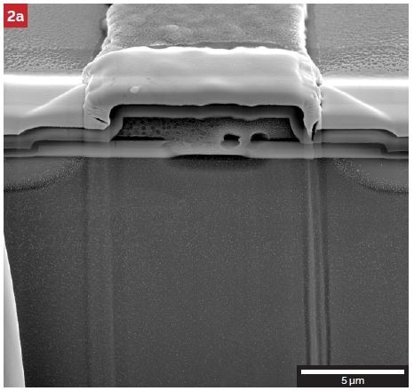
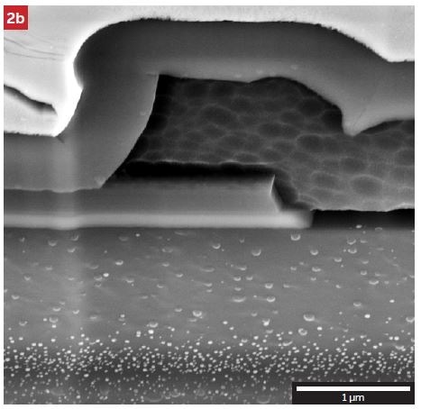
Figure 2. (a) Detailed image showing visualized active areas. (b) The higher magnification image for intricate inspection.
Conclusion
Plasma FIB provides a reliable solution for the inspection and visualization of oxide and diffusion layers, compared to existing technology, considering aspects such as accuracy, speed, reliability and likelihood of sample damage occurring. Furthermore, using the Plasma FIB enables site-specific inspection with the possibility of precise navigation to a specific ROI. These benefits make plasma FIB an ideal tool for efficient inspection during the manufacturing of semiconductor devices.
Acknowledgements
Images courtesy of ON Semiconductor, Rožnov pod Radhoštěm. The installation and operation of a dedicated FERA3 Plasma FIB/SEM system in the ON Semiconductor facilities is supported by the Technological Agency of the Czech Republic; grant no. TE 01020233 (AmiSpec).
TESCAN Group
Founded in 1991 by a group of managers and engineers from Tesla with its electron microscopy history starting in the 1950’s, today TESCAN is a globally renowned supplier of Focused Ion Beam workstations, Scanning Electron Microscopes and Optical Microscopes. TESCAN’s innovative solutions and collaborative nature with its customers have won it a leading position in the world of nano- and microtechnology. The company is proud to participate in premier research projects with prominent institutions across a range of scientific fields. TESCAN provides its clients with leading-class products in terms of value, quality and reliability. TESCAN Group is the North American arm of TESCAN Group, a multinational company established by the merger of Czech company TESCAN, a leading global supplier of SEMs and Focused Ion Beam workstations, and the French company ORSAY PHYSICS, a world leader in customized Focused Ion Beam and Electron Beam technology.

This information has been sourced, reviewed and adapted from materials provided by TESCAN Group.
For more information on this source, please visit TESCAN Group.