The key to understanding how a material will respond to specific conditions is a complete analysis of its properties. As well as the compositional and structural information offered by FIB-SEM and SEM imaging and analysis, Electron Backscatter Diffraction (EBSD) can reveal crystallographic phases and their distribution. It also provides information about grain orientation.
EBSD utilizes electron-backscattered diffraction patterns to show a material’s crystallography. When an SEM column electron engages with the atoms of a material, it inelastically scatters some electrons, resulting in a divergent source of low-energy electrons near the surface of the sample. EBSD patterns are then formed using these electrons. For successful EBSD analysis, a deformation-free material surface is required to attain the required yield of the electrons.
Preparing samples for EBSD analysis can be difficult, particularly for materials that are sensitive to the polishing beam energy, or materials with multiple phases of varying hardness.
Mechanical polishing is one option. While this method is well suited for many materials, it is unable to attain the surface quality required for multi-phase or sensitive materials, as the softer phase is more easily removed, leading to one phase being over-polished. Mechanical polishing is also unsuitable for materials that recrystallize and transform into different phases, such as duplex steel.
A second option is electrochemical polishing; however, it too has some material restrictions. Balancing polishing efficiency for materials with more phases and different chemical compositions can therefore be difficult.
Ion polishing methods facilitate the application of various ion beam energies to limit deformation on the sample’s surface. Removal of the top surface produces a pristine material surface for analysis. This study investigates the use of TESCAN’s Low Angle Polishing technique for the preparation of multi-phase materials for EBSD.
A combination of Low Angle Polishing technique and plasma FIB allows the processing of large areas, offering data from a larger area, and improving the size of the statistical sampling for greater accuracy in the conclusions drawn about a material.
Materials and Methods
Three materials were prepared and characterized. The first sample was duplex steel, and the second and third samples were from the WC-Co materials group.
A TESCAN AMBER X plasma FIB-SEM was utilized for the material polishing as well as the EBSD analyses. The instrument was equipped with an EBSD camera from Oxford Instruments and TESCAN’s patented Low Angle Polishing method was used to polish large areas of each sample.
TESCAN developed and patented this method primarily for applications in the semiconductor industry; however, it can also yield high-quality uniform surfaces on materials science samples that are otherwise difficult to polish.
To reduce damage to the sample surface, the Low Angle Polishing method employs low ion incident angles. The whole process is controlled using the EssenceTM Low Angle Polishing software module, which automates adjustments of the sample’s surface position to reduce the creation of polishing artifacts. It also supports seamless switching between beam energies throughout the polishing process, allowing for the use of the lower ion energies as required.
FIB polishing was initially performed using a FIB current of 30 nA. The ion beam energy was set to 30 keV, 15 keV, and 10 keV respectively. In the second experiment, the ion beam setting was 30 keV and 100 nA, and 15 keV and 75 nA were used to evaluate the dependency of EBSD pattern quality on ion beam current.
EBSD datasets were collected using a 20 keV and 10 nA electron beam. High-resolution mapping, even at high beam currents, was attained via the automated beam profile adjustment, a standard feature of TESCAN microscopes.
Results and Discussion
The Low Angle Polishing method was highly effective at producing high-quality, uniform surfaces for EBSD characterization. Combining the Low Angle Polishing method with plasma FIB-SEM expands the technique to the preparation of large-area surfaces. Figure 1 illustrates the duplex steel sample with a polished area of 500 μm x 500 μm. The final polishing was conducted with the Xe plasma FIB utilizing 10 keV at 30 nA.
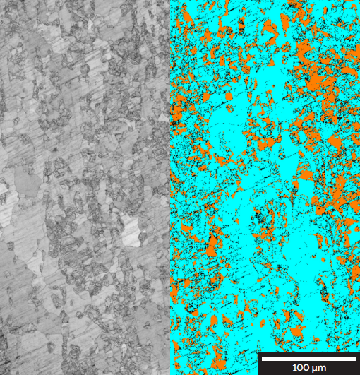
Figure 1. The large area of 500 μm x 500 μm EBSD map from the surface polished by Low Angle Polishing method shows band contrast image (left) and phase distribution map (right). Image Credit: Tescan USA Inc.
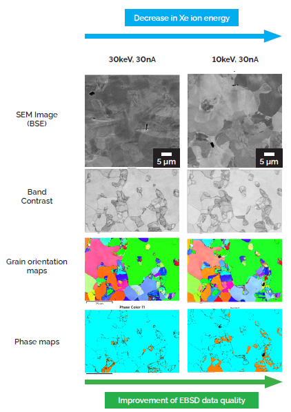
Figure 2. A comparison table showing the improved quality of EBSD data following the implementation of reduced ion beam energy during polishing. Image Credit: Tescan USA Inc.
Decreasing the ion beam energy led to improved surface quality, as shown in Figure 2. The table shows a comparison between the SEM images, band contrast, and Inverse pole figure (IPF) images demonstrating the phase distribution map and grain orientation map.
The BSE image of the sample polished at 10 keV offers further channeling contrast for the depiction of the grain structure information. The EBSD results highlight a small improvement in indexing from 2.5 zero solutions to 2.4 zero solutions.
When comparing the two-phase maps, an important difference is observed. Both maps were obtained from the same location on the sample. As a result of the polishing, part of the material was removed, and therefore the z position differs. Thus, it cannot be claimed that the lower energy blocks the material recrystallization. However, more FCC phase can be detected in a material after polishing at 10 keV. This effect can additionally be explained by superior indexing caused by improved EBSD pattern quality (shown in Figure 3).
The amount of FCC phase increased from 2.06 % (when the sample was polished by 30 keV ion beam energy) to 6.91 % (after being polished by 10 keV). The zero solution was kept relatively similar, changing from 2.52 % to 2.35 % while the ion energy decreased.
This behavior was also observed on the WC-Co material (Figure 4). Reducing the beam energy resulted in an increase in grain channeling contrast, simultaneous improvement in phase indexing, and improvement in band contrast. It can be considered that the total area of grain boundaries found in a sample will remain consistent from a statistical perspective.
It can also be assumed that the better indexing is a result of the improved EBSD pattern, which positively impacts the indexing quality. The indexing improves by 9.5 % zero solution for the 15 keV polishing step, 10.1 % zero solution for the surface polished at 30 keV, and 8.2% zero solution for index quality from the surface polished by 10 keV beam energy.
The effect of ion beam energy on the surface quality of the sample was investigated on a second similar sample from the WC-Co materials group. In Figure 5, the pattern quality created by different polishing conditions for each of the phases found in the material is shown. Polishing conditions vary from 30 keV at 100 nA, 30 keV at 30 nA, 15 keV at 75 nA, and 10 keV at 35 nA. The acquisition time of a single pattern was 5 ms for the surface processed at 30 keV at 100nA and 8 ms for the remainder of the milling conditions.
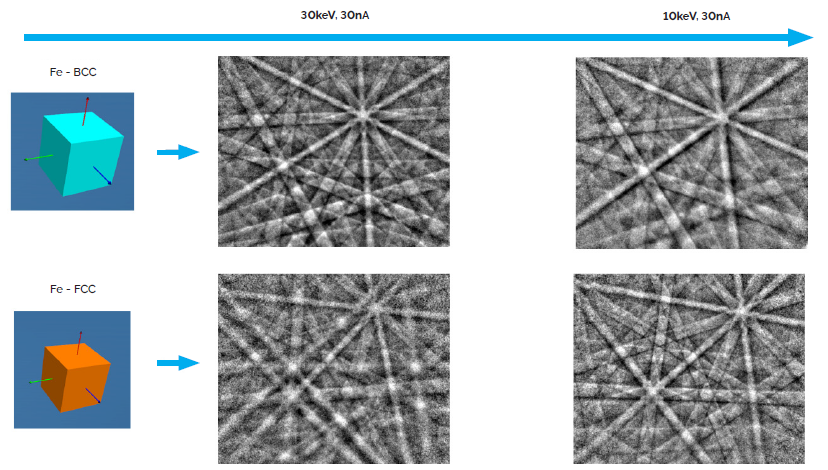
Figure 3. Corresponding EBSD patterns for the two phases of duplex steel polished at 30 keV and 10 keV with a beam current of 30 nA. Image Credit: Tescan USA Inc.
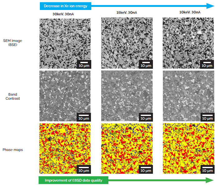
Figure 4. A comparison table showing the difference in the quality of EBSD data after polishing at decreased Xe plasma FIB beam energies. Image Credit: Tescan USA Inc.
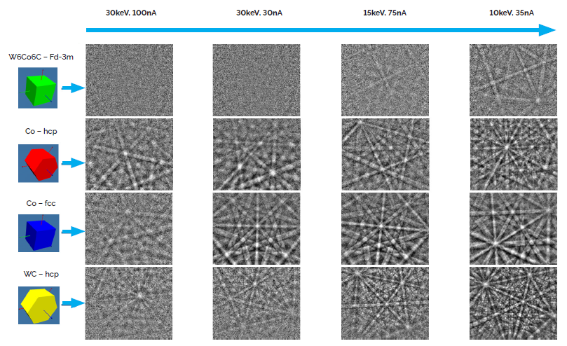
Figure 5. EBSD pattern phases were detected in WC-Co cutting material polished at different ion beam conditions:30 keV 100nA; 30 keV 30nA; 15 keV 75nA and 10 keV of 30 nA. Image Credit: Tescan USA Inc.
The data in Figure 5 demonstrates the pattern improvements related to the beam energy and the ion beam current. The lower energies are of benefit for high-resolution EBSD mapping when the high-quality EBSD pattern is mandatory, or to polish samples that contain different phases or are sensitive to high energies.
Conclusion and Outlook
Low Angle Polishing is a ubiquitous polishing method that can be useful in EBSD sample characterization. The method is also suitable for materials that are challenging to polish utilizing traditional methods, such as mechanical polishing, as it reduces surface damage and the creation of curtaining artifacts.
TESCAN EssenceTM software automates a part of the polishing process. The EssenceTM Low Angle Polishing software module allows the utilization of a variety of ion beam settings. The capability to adjust ion beam settings for Low Angle Polishing is critical when samples are difficult to polish because they contain multiple phases with varying hardness. By implementing the Low Angle Polishing method on Plasma FIB-SEM, large area polishing is enabled, allowing researchers to characterize a more statistically relevant sized sample.

This information has been sourced, reviewed and adapted from materials provided by TESCAN USA Inc.
For more information on this source, please visit TESCAN USA Inc.