Wood is a natural material with a long history of practical use. It is used in a wide variety of applications ranging from children’s toys right through to the development of wooden skyscrapers in places like Australia or Canada.
Observing Wood Specimens in their Natural Uncoated State
Wood has a number of natural advantages, making it a particularly unique material. These include a high strength-to-density ratio, the consumption of CO2 during its growth, and a complex microstructure which is utilized in bio-inspired engineering.
Wood is a non-conductive material. This means that in order to observe its microstructure using scanning electron microscopy (SEM), any samples must be sputter-coated with a very thin layer of noble metals (for examples Pt or Au) in order to prevent charging artifacts during imaging.
Limitations of Scanning Electron Microscopy
This technique is, however, not without its disadvantages. A key problem is that even coating layers of just a few nanometers can disguise nano-sized features on the sample’s surface, in some cases even hiding them entirely. It also has the potential to fill voids in some structures, for example, margo in bordered pits.
In order to circumvent this particular problem, it is possible to observe specimens under low vacuum conditions, though this does have the drawback that the sample may be observed in a lower resolution, therefore making it harder to suitably resolve any nano-scale features on the sample’s surface.
A further option would be the use of low voltage imaging to avoid charging, but this would compromise the signal throughput, also causing image resolution to be reduced.
It is a better option therefore to observe wood specimens in their natural uncoated state, and also at a high vacuum. This ensures maximum resolving power.
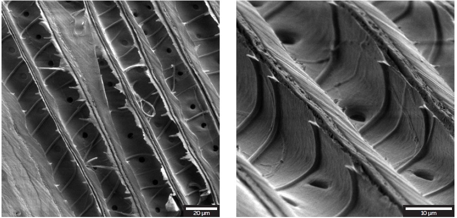
Figure 1. Longitudinal cross-section through a spiral thickened cell-wall of the sample (left). Higher magnification of the sample tilted at 55° (right).
TESCAN S8000 Microscope
These difficulties are comprehensively overcome by the TESCAN S8000 microscope as it delivers uncompromised ultra-high resolution (UHR) imaging, even at low beam intensities.
Fitted with the BrightBeam™ SEM column, they are able to offer field-free UHR, operating with an extended electron beam energy that ranges from 50 eV to 30 keV.
The S8000 microscope is fitted with an E-T detector that has been optimized for maximum signal collection at low beam intensities. It is, therefore, able to deliver excellent topographical contrast, even when working in the ultra-low beam energy range.
Overall, these impressive capabilities combine to make the S8000 microscope a perfect instrument for the observation of nanostructures within uncoated wood or wood-like specimens, for example; plants, paper, or wooden fibers.
The images presented below were acquired with the S8000 microscope using the E-T detector and electron beam energy of 500 eV. The sample itself is Yew (Taxus baccata).
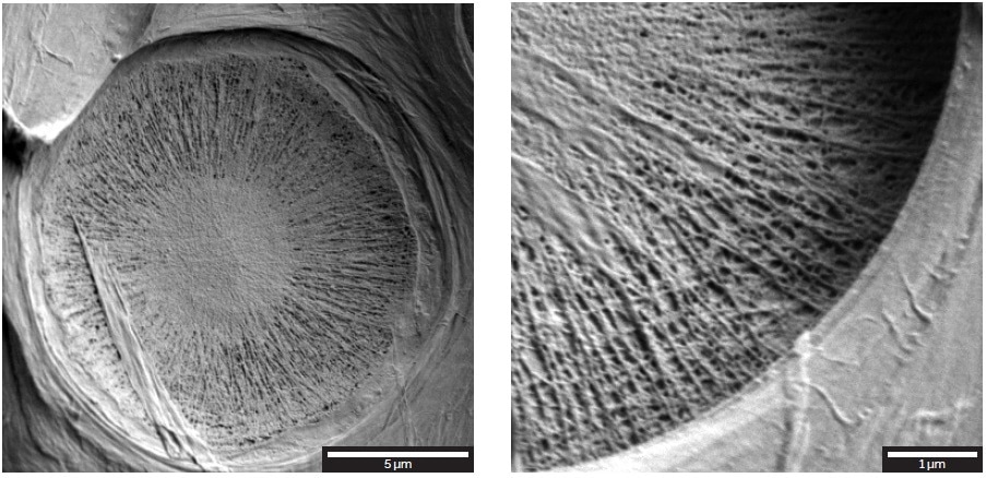
Figure 2. Overview of a bordered pit with torus and membrane of the sample (left). Higher magnification of the sample tilted at 55° (right).
TESCAN Group
Founded in 1991 by a group of managers and engineers from Tesla with its electron microscopy history starting in the 1950’s, today TESCAN is a globally renowned supplier of Focused Ion Beam workstations, Scanning Electron Microscopes and Optical Microscopes. TESCAN’s innovative solutions and collaborative nature with its customers have won it a leading position in the world of nano- and microtechnology. The company is proud to participate in premier research projects with prominent institutions across a range of scientific fields. TESCAN provides its clients with leading-class products in terms of value, quality and reliability. TESCAN Group is the North American arm of TESCAN Group, a multinational company established by the merger of Czech company TESCAN, a leading global supplier of SEMs and Focused Ion Beam workstations, and the French company ORSAY PHYSICS, a world leader in customized Focused Ion Beam and Electron Beam technology.

This information has been sourced, reviewed and adapted from materials provided by TESCAN Group.
For more information on this source, please visit TESCAN Group.