Optical characterization of MEMS devices can be performed by using an extensive range of measurement systems. These follow different technologies at hand for the measurement of various physical properties (for example, cross-section, dimension, roughness, film thickness, modulus elasticity, step height, response time, stress, resonance frequency, thermal expansion, stiction, etc.).
For instance, dimensional analysis and measurement of deformations can be performed by basic optical microscopy with digital image processing.
More sophisticated optical measurement systems are customized for particular capabilities (high lateral resolution, 3D shape measurement, high vertical resolution, and/or dynamic response). A comparison of methodologies commonly available for this purpose is illustrated in Table 1.
Table 1. Comparison of MEMS optical measurement tools
| Technique |
Lateral Resolution (typical) |
Vertical Resolution (typical) |
Static Shape |
Dynamic Response |
Realtime Response |
| AFM (Atomic Force Microscopy) |
0.0001 µm |
0.0001 µm |
3D |
No |
No |
| SEM (Scanning Electron Microscope) |
0.001 µm |
- |
2D |
No* |
No |
| OM (Optical Microscopy) |
<1 µm |
<1 µm |
2D |
No* |
No |
| CM (Confocal Microscopy) |
<1 µm |
<0.01 µm |
3D |
No |
No |
| WLI (White-light Interferometer) |
<1 µm
<0.01 µm ** |
<0.001 µm |
3D |
Yes** |
No |
| DHM (Digital Holographic Microscopy) |
<1 µm
<0.01 µm ** |
<0.001 µm |
3D |
Yes** |
No |
| SVM (Strobe Video Microscopy) |
<1 µm
<0.01 µm ** |
<1 µm |
2D |
Yes** |
No |
| LDV (Laser Doppler Vibrometry) |
<1 µm
<10-6 µm *** |
<10-6 µm *** |
No |
Yes |
Yes |
*Dynamic response possible using video capture technique
**Dynamic response possible using strobe technique
***Resolution for real-time dynamic response — not static
A laser Doppler vibrometer’s (LDV) real-time capability enables measurement times roughly six orders of magnitude smaller compared to any method that is based on strobe techniques or provides a comparable measurement time and an amplitude resolution of roughly six orders of magnitude or even better.
Polytec Optical Measurement System
Polytec’s optical measurement system is a specialized system developed for the measurement of dynamic response. Generally, in MEMS devices, elements for sensing and actuation are actively moved. Measurements of dynamic response offer crucial information that cannot be obtained by just electrical testing. Settling displacement amplitudes of resonators, time dynamics of micro-mirrors, and resonance frequency of cantilevers are some examples of dynamic response measurements. In this case, high-resolution, real-time, and precise non-invasive measurement techniques are required.
The Polytec microscope-based measurement system uses the following three technologies: (1) Out-of-plane motion is measured by laser Doppler Vibrometry. In-plane motion measurements are performed by incorporating two additional vibrometer channels that are angled to the surface. It is possible to measure and display deflection shapes as 3D animations by automated scanning. (2) Another method for measuring in-plane motions is strobe video microscopy, which again extends the analysis to the planar direction to offer a complete 3D motion measurement. (3) White-light interferometry (WLI) adds the potential of surface topography measurement for measuring static shape.
Currently, this instrumentation is being adopted by the entire MEMS community for the characterization of devices such as accelerometers, micro-mirrors, gyros, cantilevers, ultrasonic transducers, actuators, microphones, RF switches, pressure sensors, ink jets, and resonators. Following are some of the applications:
- Characterizing device response at the time of design development and release processes
- Dynamic testing of device response to establishing mechanical parameters like stiffness, resonant frequency, and damping
- Calibrating of displacements of sensor and actuator against drive voltage over an extensive range of motion and frequencies
- Design validation of performance against expected predictions of FE model
- Topography measurement to establish surface properties following fabrication process (roughness, shape, step height, geometry, film stress, curvature, delamination)
- Measuring settling time dynamics to establish precise movement against time and to display 3D visualization of response
This article gives a detailed account of the way in which the Polytec optical measurement system is used for many of these examples. The principles of operation are crucial for gaining insights into the intrinsic advantages and disadvantages of the technology employed. An elaborate outline of this technology is given in the following sections, with examples illustrating how the aforementioned methods are used for important applications.
Laser Doppler Vibrometry
The LDV is an optical instrument that employs laser technology to evaluate displacement and velocity at chosen points on a vibrating structure. Laser vibrometers perform measurements without contact and are not influenced by environmental conditions or surface characteristics. It is possible to focus the laser beam to a spot down to 1 µm in diameter, thereby enabling analysis of MEMS structures that are visible under an optical microscope.
Diffraction limitations affect measurements of devices with a size smaller compared to the wavelength of the used light (532 nm). LDV is an extremely sensitive optical method with the overall potential of evaluating displacements from centimeters to picometers at frequencies from near DC to gigahertz. Apart from their broad frequency range, LDVs also have a wide dynamic range (more than 170 dB) for velocity amplitudes of 0.02 µm/s to 10 m/s. These attributes enable measurements that cannot be performed using holographic or other methods.
The LDV employs the Doppler effect in which information related to the motion quantities, displacement, and velocity at the point of incidence is carried by the light backscattered from the moving target. The phase of the light wave is modulated by the displacement of the surface while the optical frequency is shifted by the instantaneous velocity. The received light wave is mixed with a reference beam with the help of interferometric methods to make the two beams to recombine at the photo-detector. Figure 1 illustrates the basic schematic structure of a modified Mach-Zehnder interferometer.
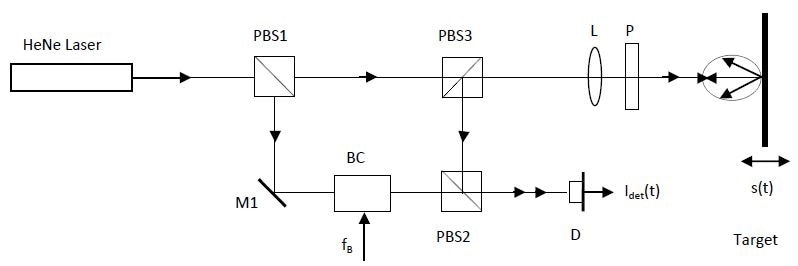
Figure 1. Optics schematic of a modified Mach-Zehnder Interferometer
Phase modulation and direction sensitive frequency from the moving target are carried by the signal measured at the photo-detector. Target displacement s(t) leads to a phase modulation
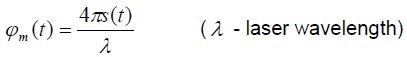 |
(1) |
The basic relationships dφ/dt = 2πf and ds/dt = v govern the phase modulation to be in correspondence with a frequency deviation called the Doppler frequency.
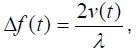 |
(2) |
The detector output signal’s resultant frequency precisely conserves the velocity vector’s directional information (sign).
By nature, the measurements carried out by LDV are dynamic and do not carry information related to the static shape (as is feasible using other methods such as white-light interferometry or digital holography). Velocity and displacement are encoded in phase and frequency modulation of the output signal of the detector. Phase and/or frequency demodulation methods are employed in a laser vibrometer’s signal decoder blocks to recover the velocity and displacement time histories from the modulated detector signal.
The instantaneous Doppler frequency is directly converted into a voltage proportional to the vibration velocity by analog and digital frequency demodulators. The high-quality demodulation electronics employed offer sensitivity, critical accuracy, signal-to-noise ratio, and linearity for the entire vibrometer system.
It is possible to extend the LDV measurement instruments to a 3D vibrometer setup, thereby enabling pm-resolution for in-plane as well as out-of-plane motion. The optical configuration is predicated on heterodyne Mach-Zehnder interferometry that includes three linearly independent interferometer paths (Figure 2).
A Bragg-cell acousto-optically frequency-shifts the laser beam directed on-axis via the main interferometer relative to the three reference beams. Then, the scattered light is collected on-axis as well as in two off-axis directions. The complete broad-bandwidth 3D vibration spectra at the measurement spot are contained in the three detector signals. The vibration data in Cartesian coordinates is derived using a coordinate transformation.
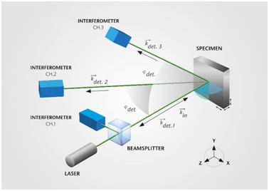
Figure 2. Optical layout of 3D laser vibrometer
One drawback of employing LDV is that the measurements are performed at a single point, in contrast to being captured on a complete field as performed using video interferometry methods. The LDV technique can be extended to full area scanning by using scanning mirrors to deflect the laser measurement beam in x and y directions.
Figure 3 illustrates the schematic for this, with scanning mirror M. It is possible to position the laser measurement beam to any point visible on the live microscope video. This method is applied to scan an area point by point to evaluate the structure’s velocity field.
Despite the fact that a single-point LDV can be regarded as a traditional sensor (i.e. recording analog output using an oscilloscope or other data acquisition systems), the scanning LDV necessitates system software to generate a scan measurement grid, to achieve scanning process control, and to simultaneously acquire the measurement data. The phase of each point is established by simultaneous measurement of an additional reference channel (usually the drive signal generated by the internal signal generator). The 3D deflection shapes are computed from this data. The final outcome includes velocity mapping and/or mapping of the displacement field over the structure that enables 3D animations of the response in the time or frequency domain (see Figures 12 and 14).
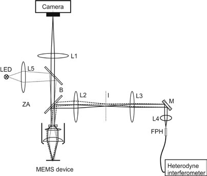
Figure 3. Optical layout of microscope scanning laser vibrometer
Strobe Video Microscopy
In-plane periodic motion of MEMS is measured using strobe video microscopy. This method can be employed together with LDV. As depicted in Figure 4, the stroboscopic images are captured by an integrated CCD camera. It is necessary to accurately synchronize the LED-strobe flashes, the signal that drives the specimen, and the camera exposure. Figure 4 illustrates a timing diagram of the strobe synchronization for two camera shots at two distinct phases with respect to the periodic excitation.
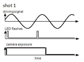
Figure 4. Timing diagram of the strobe signals
After acquiring a data set containing strobe images, pixel deviations between frames are established through machine vision analysis. In-plane motion algorithms use correlation functions to compute the position shifts (δx, δy) of a user-defined search pattern between successive images. Image-correlation methods can be used to calculate the values of δx and δy down to sub-pixel resolution. This necessitates post-processing and is not captured in real-time, as is the case with the LDV.
The displacement and pattern match of a comb drive MEMS device at resonance are shown in Figure 5. The system automatically steps via user-defined frequencies, and frequency response is obtained by recording image sets. For each measured frequency, displacement versus phase delay data is extracted and presented as a Bode plot. In-plane motion analysis can be carried out with sine excitation as well as for a step response.
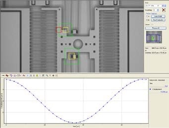
Figure 5. In-plane motion of comb drive device
White-Light Interferometry
White-light interferometry (WLI) enables static surface topography measurements. This offers x-y-z mapping of the surface of the device to establish important parameters such as step heights, flatness, parallelism, curvature, angles, roughness, and volumes. It is possible to display the result as 2D or 3D mappings for defect analysis, assessment, and/or processing to extract parameter values for specified areas.
WLI is performed using a Michelson interferometer by adopting the optical setup illustrated in Figure 6. The coherence length of the white-light source employed is in the micrometer range. A beam splitter is used for splitting the collimated light beam into a reference beam and an object beam. The light scattered back from the object and the mirror is superimposed at the beam splitter once more and imaged to the CCD camera. This interference leads to a fringe pattern that is mapped out for every pixel in the camera image.
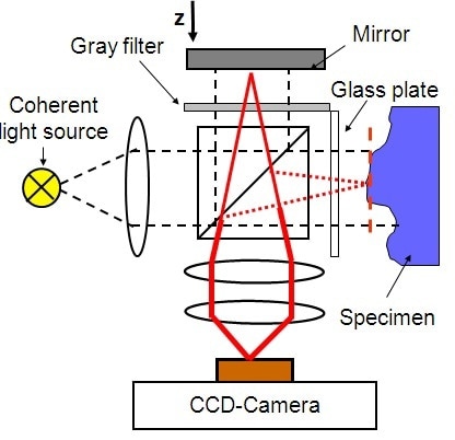
Figure 6. White-light interferometer schematic
A z-stage is used to move the position interference lens, thereby modulating the interference signal for every pixel, resulting in a correlogram. The maximum value of the correlogram appears when the distance to the reference mirror is precisely equal to the distance to the device surface. Following a measurement run, the correlograms obtained from the camera frames are analyzed, and as illustrated in Figure 7, it is possible to reconstruct a true topographical representation of the surface as a 3D topography map.
Figure 7. Topography measurement of a micro gearwheel
Application — Texas Instruments Digital Mirror Device (DMD)
Settling time is a key parameter for the micro-mirror applications in which mirror orientation is quickly switched from one tilt state to another. In this case, accuracy and speed are important performance indicators. The settling time response is affected by complex factors in the mirror design like resonance frequencies, damping coefficients, and optimization of drive control signals. Laser Doppler vibrometry can be used to measure these factors for real-time response with high accuracy and sampling rate. 3D visualization of mirror response is offered by scan measurements as time animated sequences.
Measurements are performed on Texas Instruments DMD arrays. The array includes millions of 12 μm mirrors. Figure 8 depicts the rotation of each mirror by ±12° about a primary axis by twisting with respect to a hidden hinge. The illumination projected for an individual pixel can be controlled by moving the mirror from “−” to “+” state, and the gray level brightness can be controlled by the amount of time at the “+” state. The mirrors have the ability to switch on/off at a rate of roughly 50,000 times per second. The range of color scales in the projected image can be increased by further improving the switching speed.
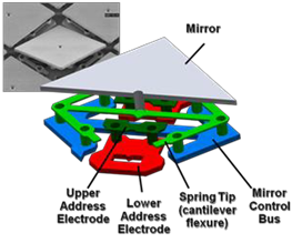
Figure 8. Structure of a Texas Instruments micro-mirror
LDV is used for performing scan measurements on the DMD array to measure settling time response and offer a 3D time visualization of movement. The displacement of a point targeted by the laser measurement spot at the corner of the mirror is illustrated in Figure 9. Upon transitioning to the “+” state by rotating 12°, the corner of the mirror is displaced upward and requires a characteristic time to settle to a stable orientation.
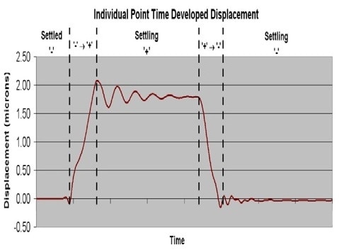
Figure 9. Time response of an individual point on a mirror
At the time of the settling, the mirror exhibits a damped oscillation at the basic torsional resonance. A complete 3D dynamic representation of the movement of the mirror can be established for the primary tilt motion, together with the orthogonal roll and sag motions, by repeating this measurement at coordinate locations over the entire surface. The outcome is a 3D animation displaying the precise time sequence for all the three axes. The relative phase of the motion from one mirror to another can be compared by extending the measurement over multiple mirrors in the array. These measurements served as a crucial gage of design settling time performance and are applied to direct future design development.
Application — Testing Pressure Sensors on Wafer Level
Wafer-level testing can offer a robust method of quality control and minimize costs associated with packaging MEMS devices that do not fulfill the specifications. The use of LDV for the identification of material and geometrical parameters enables real-time measurements that can be rapidly automated at the wafer level on a probe station.
The measurement microscope head used can be easily mounted on any probe station. It is possible to measure the resonance frequency at a single point on the structure within a few milliseconds. The probe station moves to the next device and the same measurement is repeated. The process requires roughly 2 seconds per die, and the final outcome is a wafer map that displays quantitative Estimated Identification Error used for “pass/fail” criteria.
Measurements are performed for pressure sensors that comprise of 1300 µm x 1300 µm devices, processed through KOH etching. A membrane thickness algorithm based on frequency response measurements performed by LDV is employed as the principle of parametric testing. Contactless electrostatic probes are used for exciting the membranes. The frequency response of two devices is shown in Figure 10: the frequency response of a “good” die that has resonances at anticipated frequencies is shown in Figure 10A, and the frequency response of a “bad” die that has shifted resonance frequencies is shown in Figure 10B.
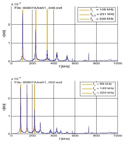
Figure 10. (A, upper): Frequency response of good device. (B, lower): Frequency response of bad device.
Calculation of an Estimated Identification Error (EIE) offers a quantitative evaluation that enables the processing errors to be classified. As illustrated in Figure 11, these are mapped on the wafer, with criteria for maximum error used for screening out “bad die” (shown in red).
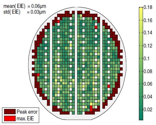
Figure 11. Wafer map of Estimated Identification Error. Bad Devices are shown in red.
Application — FE model validation
Simulation of the mechanical response is performed by using FE models during the design phase of MEMS devices. In typical models, complex mechanical and electrical parameters are employed to predict device response and are used to design the device based on target specifications. Due to the fact that several of these parameters have variations because of fabrication processes, it is vital to validate them by testing. This specifically holds good at the initial fabrication phases in which the process is not well controlled and there are more uncertainties.
Described below is a basic example of a MEMS cantilever beam. The length of the silicon beam is 225 μm, with a width of 40 μm and a thickness of 4 μm. The resonance frequency f is given by
 |
(3) |
where L is the length, m is the mass, I is the moment of inertia, and E is the elasticity. An ANSYS model of the silicon beam is extracted using 1000 node points based on the modeled geometry. It is predicted that the first bending mode will occur at 94,153 Hz (see Figure 12, right). This model is experimentally validated using scanning LDV measurements on the beam, with the measurement points density same as that of the node points for the model.
Comparison of the experimental results is performed for validation and the model is updated on the basis of the data. In an idealized model, complex effects like damping, geometric errors, mismatching boundary conditions, non-uniformities, torsional compliance, and residual stress are usually not taken into consideration. Here, the first bending mode is provided by the experimental results, at a lower frequency of 66,718 Hz (see Figure 12, left). Inaccurate geometrical values used in the model offer an explanation for this.
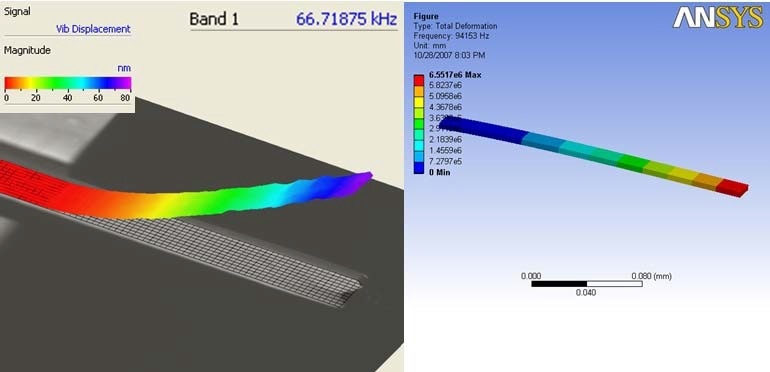
Figure 12. Comparison of cantilever first bending mode determined experimentally (left) and from FE model (right).
In the case of inertial sensors, modeling could be much more complex for sense and drive modes using, for instance, tuning fork or comb drive resonators. These modes are generally designed at particular frequencies that must be validated by performing experimental measurements.
Application — Optimizing the Design of Accelerometers
MEMS devices are designed with integrated mechanical and electrical components to form electro-mechanical systems. During the characterization and troubleshooting of these devices, it is usually challenging to establish whether a behavior observed is absolutely electrical, absolutely mechanical, or intrinsically both. LDV measurements enable direct mechanical measurements unaffected by electrical effects.
An example measurement is illustrated for a robust, stable MEMS low-g servo accelerometer earlier manufactured by Applied MEMS. The noise floor of the accelerometer is close to 30 ng/√Hz and its dynamic range is >115 dB. Although the sensor is designed to suit demanding environments of oil exploration for seismic exploration and monitoring, it can also be used for inertial navigation, and for vibration monitoring and analysis.
A spurious resonance is observed close to 20 kHz in the output of the accelerometer in the early stages of development. Despite the fact that this frequency is fully outside of the desired performance band, this mode is presumed to be the reason for the decrease in sensor performance. Although the source of the mode is currently obscure, there are various presumed causes. From FEA simulation, it is known that mechanical sensor modes close to this frequency exist; however, it is not clear how these modes could manifest in the sensor’s closed-loop output. Artifacts from the control loop and package-induced modes are also regarded as a source of the 20 kHz tone.
Further analyses of the cause of the tone are performed by using scanning vibrometry to scan the surface of the bare die, as illustrated in Figure 13. As the device is a variable capacitor including forcing and sensing electrodes on both sides of the moving proof mass, it was necessary to remove one of the electrode caps to scan the moving parts inside. The de-capped die, which is secured to a high-frequency shaker, is mechanically stimulated in the band of interest.
The broadband input to the shaker is used to scan the complete surface, to excite all modes in the band of interest. Through this step, the frequency and general location of the modes for the device under test were revealed. This information can be used for performing higher resolution fast scans at single frequencies, for particular modes at different locations on the die.
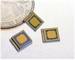
Figure 13. MEMS accelerometer die from Applied MEMS
Figure 14 illustrates the results of a fast scan over a 1.5 x 1.5 mm section that contains the accelerometer spring elbow. The spring elbow’s peak displacement is 800 nm. From the scan, a mechanical resonance of the spring elbow can be clearly seen. Since only mechanical excitation adopted to perform the LDV measurement, it is possible to further eliminate the electrical causes of the spurious mode. Additional higher-order modes of the spring arm at frequencies close to 1 MHz are also revealed by the scan. Consequently, the negative effects of this mode are reduced by redesigning the sensor. The subsequent sensor designs result in higher yields and optimized device performance.
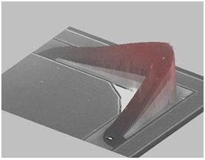
Figure 14. Bending mode of flexure at 23 KHz
Conclusion
The versatile optical measurement tools offered by Polytec can be used for the research and development of MEMS devices that are used in real-world applications. Laser Doppler vibrometry enables broadband measurements of dynamic response to be performed in real time, with a resolution down to the picometer level. The examples discussed in this article illustrate its usage for the characterization, design optimization, and troubleshooting of the Texas Instruments DMD array and applied MEMS accelerometer.
Furthermore, it is possible to extend this potential to automated, fast production test measurement on the wafer level. The application of Polytec’s measurement methods offers unique insights into the inner workings of MEMS devices, enhances yield and performance, shortens design cycles, and eventually decreases the cost of the product.

This information has been sourced, reviewed and adapted from materials provided by Polytec.
For more information on this source, please visit Polytec.