This article considers different photoresist materials, their utilization in the semiconductor industry, and different photoresist coating methods.
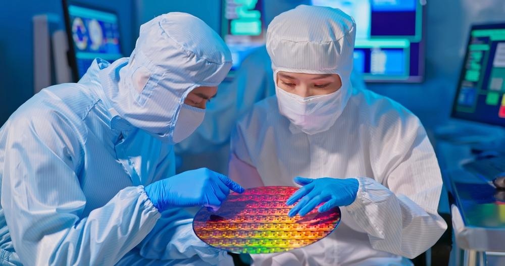
Image Credit: aslysun/Shutterstock.com
Semiconductors could be termed as the most extensively utilized substance in the modern century owing to their vast advantages over their counterparts. Modern computers, the transportation industry, the telecommunication sector, electronics, as well as commercial and military hardware all use semiconductors.
Polycrystalline wafers are used to make semiconductors. A single 300-mm silicon wafer may create hundreds of chips. Photoresist coatings and materials are an essential part of their fabrication as they are the main constituents of the photolithography process during the fabrication of the semiconductors.
It is a micro-synthesis technique involving the use of photoresist chemicals for transferring geometric patterns onto the semiconductor substrate or films. During the photolithography phases of photoresist administration, advancement, and stripping, photoresist chemicals are released.
Introduction to Photoresist Materials
A photoresist is a light-sensitive substance that is used to generate a structured covering on a substrate in a variety of procedures such as photolithography. They are made up of polymers, sensitizers, and solvents. Each element serves a specific purpose. When exposed to radiation, the polymer's structure undergoes a modification.
The solvent enables the photoresist to be twisted and thin layers to form on the silicon wafer. Finally, the sensitizer, also known as an inhibitor, regulates the photochemical process in the polymer network.
Types of Photoresists Utilized in the Semiconductor Industry
Two distinct photoresists are utilized in semiconductor fabrication during photolithography. They are termed positive and negative photoresists.
Positive photoresists are compounds that become more absorbent after being exposed to radiation. A photoactive chemical, substrate resins, natural carrier solvents, stabilizers, polymerization blockers, viscosity control chemicals, dyes, and plasticizers are all included in these photoresists.
Negative photoresists are material coatings that crosslink and become intractable in developing fluids when exposed to radiation. Polyisoprene can be found in a variety of negative photoresists. These photoresists are made up of photosensitive chemicals, non-photosensitive chemicals, and carrier fluids. For photosensitive materials, azides are frequently used in negative photoresists. Positive photoresists are the most common in manufacturing. Poly alkyl aldehyde, isoprene, and polymethacrylate are currently employed as photoresists.
What are Different Photoresist Coating Techniques on Semiconductors?
Each photoresist-related technique necessitates the use of a resist layer of a specific thickness on a specific foundation molecule. The essential factors that determine the process to be used for this purpose include required film thickness, the topology of the substrate, and photoresist material type. The famous methods include spin coating, spray coating, dip coating, and roller coating.
Spin coating is the most widely used spraying process, at least in nanoelectronics, due to its high resist layer thickness uniformity and quick coating periods. Due to the severe air disruptions, the resist develops a noticeable edge bead around the platform margins in the case of non-rotation-symmetric substrates.
More from AZoM: Lithography Machines and the Chip-Making Process
Spray coating is another widely utilized technique in place of spin coating. Spray coating may be used on any variable dimensioned material. Resist can be sprayed on three-dimensional bodies (when properly fitted). Substrates with distinct morphology are also easily spray-coated, and high edge penetration may be achieved under optimal conditions.
However, because the resist layer is formed by thousands of droplets, the film roughness is relatively high if the droplets lose quite so much solvent throughout travel. Because the resist has to flow a little over the platform before drying in order to change from spherical to a flat sheet, it strives to decrease its volume and disengages from boundaries. There is always a trade-off between resist film cleanliness and border penetration.
Latest Research
A research article has been published in Nanoscale Advances focusing on a novel photoresist material coating. A customized quantum dot photoresist made of an organic-inorganic hybrid coating layer has been proposed. Quantum dots (QDs) are electronic nanocrystals with a nanostructured framework, a dimension of 2–10 nm, and outstanding optical features such as simple wavelength control due to the tunable size and limited full width at half maximum (FWMH) of the emission spectra. During the research, the QD photoresist employed in photolithography was a combination of QDs and a photosensitive nano-silica acrylate ceramer.
Two types of super-coaters have been suggested, based on the silica/acrylate mixing ratio: SC1230 and SC1320. The QD-PR was employed as a negative photoresist in this work. The free electrons created by the photoinitiator interacted with the acrylate in the exposed area, curing the QD-PR.
A red QD-PR released a clear unbroken red light at 10% weight under a 50 mm thickness, whereas a green QD-PR generated a clear green signal at 40% weight under the same width. If the wt. percent of the QDs and the procedure can be adjusted to lower this diameter, the results are likely to find uses in QD display devices. Furthermore, the objective of this work was more of a presentation of QD screen technology by exciting specimens of the full pixel patterns using 365 nm LEDs.
Future Perspective
Low k1 lithographic methods are necessary to enhance semiconductor technology as semi-conductor component sizes keep reducing. Improvements in optoelectronic devices and imaging capabilities, as well as advancements in EUV materials and photoresist coatings and materials, are critical for achieving true resolution enhancements and are the center of research.
In short, many advances are being done in the field of photoresist coatings and their applications in semiconductor applications paving the way for future applications.
References and Further Reading
Myeong, Seungmin, et al. 2022. Quantum dot photolithography using a quantum dot photoresist composed of an organic-inorganic hybrid coating layer. Nanoscale Advances. Available at: https://pubs.rsc.org/en/content/articlelanding/2022/NA/D1NA00744K
GAO, Jia-Xing, et al. 2021. Research Progress on High-Resolution Extreme Ultraviolet Photoresist." Chinese Journal of Applied Chemistry 38(9). 1138.
Santaclara, Jara Garcia, et al. 2021. Today’s scorecard for tomorrow’s photoresist: progress and outlook towards High-NA EUV lithography. Advances in Patterning Materials and Processes XXXVIII. Vol. 11612. International Society for Optics and Photonics. Available at: https://www.spiedigitallibrary.org/conference-proceedings-of-spie/11612/2586645/Todays-scorecard-for-tomorrows-photoresist--progress-and-outlook-towards/10.1117/12.2586645.short?SSO=1
Wang, Jiantao, et al. 2021. Photoresist Material Gap Filling Loading Improvement from Pattern Density Perspective. International Workshop on Advanced Patterning Solutions (IWAPS). IEEE, 2021. Available at: https://ieeexplore.ieee.org/document/9671257
Disclaimer: The views expressed here are those of the author expressed in their private capacity and do not necessarily represent the views of AZoM.com Limited T/A AZoNetwork the owner and operator of this website. This disclaimer forms part of the Terms and conditions of use of this website.