The imaging of nano-materials and composites is increasing in importance and therefore the role of detecting the smallest compositional differences in materials is becoming progressively more significant. Due to the high depth penetration of electrons in classical BSE (backscattered electron) imaging at high landing energies, this technology is not suitable to image nano-compositional materials with very small compositional differences.
Electrons penetrate and diffuse deeply into materials at high landing energies. The lower the density of the material, the higher the penetration. This has the potential to make nano-particles and nano-layers "invisible" due to the large scattering volume. Therefore there is a demand for a new detection principle, able to meet the challenge of imaging against the background of these requirements.
GEMINI Lens with Beam Booster from Carl Zeiss
Below a landing energy of 4 kV, the back-scatter coefficient becomes non-linear and reduces with increasing atomic number more strongly than is the case with elements with low atomic numbers. This behaviour is described elsewhere and is not the subject of this note. However, at a particular landing energy there is an equilibrium of different scattering mechanisms and no contrast is observed. When confronted with the problem that the mean free path length of BSEs from low-density materials such as proteins or polymers becomes extremely small, we have introduced new technologies to make these small signals visible. The most important item of technology in achieving this requirement is the GEMINI® lens with integrated beam booster.
Independently of the required landing energy, the beam booster maintains the electron probe at a high energy level over the full length of the column. This essential design detail means the brightness of the electron probe is maintained at low energies and an amplification of the electron signal is achieved in the reverse ray path into the column. Furthermore, the highest detection efficiency is achieved by direct detection of the BSE signal on a detector (see Fig. 1) and not by converting the BSE into SE3 as in some e x B detection systems offered in the market-place. These show only high density differences and not the fine contrast differentiation described in this article.
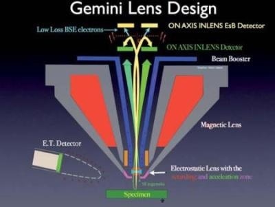
Figure 1. Schematic of the GEMINI® on axis detection principles
Since the GEMINI® lens with beam booster has a strong dispersion in the reverse imaging plane, the SEs and higher energy BSEs are separated in real time and are projected towards the individual detectors. This allows a clear separation between secondary and back-scattered electrons.
In front of the entry system on the axis of the BSE detector, is a energy filtering grid integrated into the electron optical detection system, that can be adjusted in its retarding potential from 0 to 1500 volts. This grid allows only BSEs with energies greater than the grid energy to be detected.
All the higher energy secondary and back-scattered electrons can be detected at 0 volts. By setting an appropriate threshold voltage to the filtering grid, electrons of a specific energy will be rejected and hence not detected. For example, a landing energy of 1 keV has been requested and the filtering grid potential is set to 900 V. This will give a resultant energy window of 100 eV for the BSE detector.
Due to the fact, that a specific energy band of BSEs is selected to image with this detector, it is named the EsB detector, or energy selective back-scatter detector. When this filter is active the signal does not consist of BSEs in the "normal" sense, but low loss BSEs (LL-BSE).
Understanding Low Loss Backscattered Electron Imaging
It is necessary to study the energy distribution of all possible scattering processes, in order to truly understand what low loss BSE imaging means. As an example, Figure 2 also shows the whole energy spectrum of the secondary and back-scattered (conventionally energies >50 eV) electrons plotted with increasing energy. Figure 2 also shows a number of defined features in the spectrum. These are from Auger electrons, multiple inelastic scattered electrons, plasmon losses and low loss events.
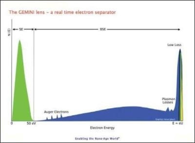
Figure 2. Spectrum of scattered electron energies from the SE process to the low loss BSE electrons
This note will focus on the sharp low loss peak at the right side of the spectrum. Figure 2 is plotted for low voltage primary beam landing energies, where the SE and LL-BSE peaks become relatively high compared to the broad saddle of multiple inelastic scattered electrons in between. The regions in the low loss peak coloured black, green and yellow represent the discrimination areas set by the filter grid voltage of the EsB detector. Of course, if the grid potential was set to a certain threshold, it would be possible just to cut off the SEs and the whole spectrum would appear blue. Under these conditions the imaging signal would have a good signal to noise ratio, but fine contrast, e.g. differentiating oxides from nitrides or complex bindings would be lost. These fine contrast differences are obtained from electrons with the smallest energy loss from a very shallow region on the surface, and not from the volume, where multiple inelastic scattered electrons are produced.
New Detection Principle
The goal of the new detection principle is the reduction of the information generated by these scattering principles, which originates from the outermost shallow region on the surface.
This technique should not be confused with the low loss BSE imaging with spectroscopic analysis performed on energy filtering TEM's, where energy losses from subelectron volts to 25 eV at most are analyzed. Such a sharp filtering process is not possible with this kind of filter used in the GEMINI® column. The aim is not spectral analysis, but merely to separate the low loss BSE electrons from the remainder of the spectrum.
Whilst operation of the EsB detector in this way enhances the contrast and increases the detection sensitivity, there is a compromise. Setting the filtering grid to discriminate to such a small information band also increases the noise. Therefore the user has to decide, how much noise contrast is required in the image or how much noise is acceptable. This is a very simple problem to solve. It is not necessary to answer the question "Which filtering grid energy do I need for detection?". It is merely necessary to go to low landing energies - to 3 keV or lower - and set the grid bias to 1500 volts. Under these circumstances an image with an energy window of 1500 eV is obtained. It is obvious that a 1500 eV energy window is a broad energy range and will also contain a large number of multiple inelastic scattered BSEs in the final image. Theses events will cause blurring and also hide some structural information due to penetration processes.
Subsequently selecting a landing energy of 800 eV and setting the grid bias to 700 V will result in a much smaller energy window of only 100 eV. In this case there is a much smaller interaction volume and only electron energies between 700 eV and 800 eV are detected.
A reduction in the landing energy will result in less electron penetration and hence more information of interest will come from the surface. With this action the mean free path length of our BSEs is also reduced and, with this, the BSE contrast.
The beam booster not only accelerates the electrons in the beam path downward, but also intercepts the electrons from the surface scattering processes and accelerates them back into the column. They are then separated from the SEs by the lens and projected directly to the EsB detector, where the separation of the LL-BSE electrons occurs in front of the filtering grid.
This backward acceleration process amplifies the signal and restores the lack of contrast back from the small backscatter coefficients, due to low atomic number elements at small landing energies. Also, no adjustment of the electron optics is necessary, when tuning the grid bias or switching between different detectors.
Advantages of Low Loss Backscattered Electrons Imaging
It makes little sense to operate at high landing energies (20 kV) while setting a grid bias to 1500 V, for large amounts of Rutherford scattering cause the loss of information and limit the detection sensitivity to 0.1 Z. The scattering volume, which is density dependent, also reduces the lateral resolution. We can therefore only see the difference of a-brass or ß-brass at high atomic numbers (Cu = 29, Zn = 30).
For low density materials with low atomic numbers, back scattering coefficients and relative atomic number values have large variability in comparison to transition elements. The conventional 0.1 Z detection limit for heavier atoms does not hold for low-Z materials in conventional BSE imaging, where the detector is below the pole piece. For light elements, the back scatter coefficient dramatically drops.
A good illustration of this effect may be obtained by comparing the following images, acquired with the GEMINI® ULTRAplus at an intermediate voltage of 12 kV with conventional BSE technology and at 1.2 kV with energy selective backscattering technology (EsB). The sample is an uncoated Perovskite rock containing almost half of the transition elements and many fluoride, chloride, oxide, and metal oxides. The images were acquired at high kV settings at 3x10^-3 mBar pressure with the charge compensation technology of the GEMINI® ULTRAplus. This relatively low pressure minimizes absorption losses from gas interactions. Nothing can be seen with 12 kV in conventional Rutherford backscattered images. This is due to the small density variations of these compounds and the relative large scattering volume in the sample. If we go to low voltage using the GEMINI® EsB Technology, filtering the low loss BSE (LL-BSE) out of the multiple inelastic electron signal, we clearly see the power of this technology. A large number of previously un-resolvable components become detectable by this method. Figure 4 dramatically illustrates how one can overlook many phases in unknown specimens, if the wrong technology is chosen.
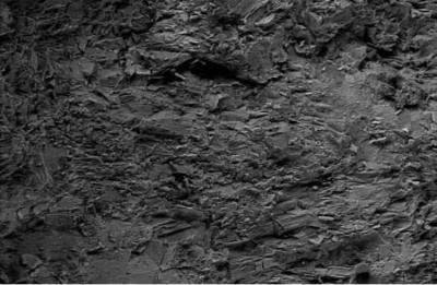
Figure 3. Uncoated Perowskite rock seen with conventional Rutherford back-scattering electrons at 12 kV
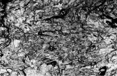
Figure 4. The same area of the Perowskite rock imaged with an EsB detector at 1.2 kV landing energy and with a window energy of 271 eV
GEMINI Technology Meeting Demands of Modern Nanotechnology
It has been seen that EsB technology with GEMINI® technology provides many advantages and is capable of meeting the demands of modern nano-technology. Also, the filtering and imaging of a selective part of the spectrum from the scattered BSEs (the LL-BSE) dramatically increase the surface detection sensitivity and compositional contrast.
By definition and because of the physical processes, the low loss BSE electrons must come from the outermost layers of the surface.
The greater the discrimination applied with the filtering grid to the smallest energy loss possible, the more the detection signal originates from the surface layers. Using this principle, the thinnest films on the surface, down to monolayers, can be imaged.
By opening the grid, reducing the filtering voltage (and hence allowing higher energy losses to be detected), deeper layers below the surface are detected. Therefore discrimination below the surface – depending on density of the material and landing energy – is possible with this principle. However, surface layers then become invisible. Obviously, since the LL-BSE interact with very shallow regions of the surface, we image with the filtered signal, an interaction volume comparable to the thin film region of a TEM sample (20 nm - 100 nm), but again: we do not spectral analyze this effect. The reduction of the net signal to the smallest energy losses increases our contrast dramatically. The fact is that these shallow interaction regions can be used to detect the smallest contrast differences between different metal oxides or nitrides, for example SiO2 or Si3N4.
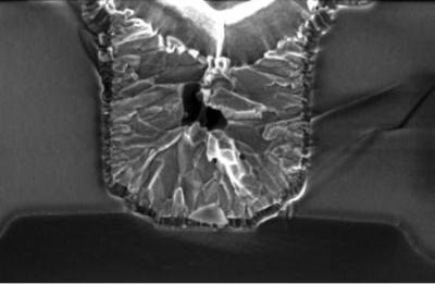
Figure 5. INLENS SE image from a sectioned semiconductor. Clearly visible: No BSE contrast!
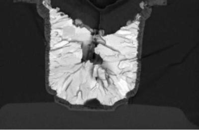
Figure 6. The same section but seen with the LL-BSE; detected with the INLENS EsB at 1.27 kV
In Figures 5 and 6, the detection power of the EsB detector can be seen as well as the clear separation of SE and BSE electrons.
Figure 6 highlights the contrast between the silicon (substrate) and Si3N4 and also Ti and TiN. This reveals a detection sensitivity that is several magnitudes greater than that of a conventional BSE detector. In many modern materials there is a requirement to differentiate between different metal oxide states or other compositional differences.
These compositions have no differences in the nuclear charge (number of protons). This is why this note refers to compositional contrast, instead of the conventionally described Z-contrast.
A possibility for the future is therefore not only the imaging of different oxidization states of metals, but also the detection of different hybridization of atoms and ligands. This topic will be a subject of a separate publication (in preparation).
Summary
To conclude there are many unique and outstanding new features in the GEMINI® column:
- Real time separation of SE electrons and BSE electrons.
- No adjustment is necessary when switching between the INLENS SE and EsB detectors.
- Simultaneous detection of 2 different signals e.g. INLENS SE and EsB.
- Direct detection of SEs and BSEs through the projection of the GEMINI® lens.
- No conversion of electrons.
- True surface imaging of SEs and BSEs through the "GEMINI® principle".
- Low loss BSE imaging through the EsB filtering technology.
- Extension of the BSE detection limits of classical 0.1 Z down to 0.001 Z or lower.

This information has been sourced, reviewed and adapted from materials provided by Carl Zeiss Microscopy GmbH.
For more information on this source, please visit Carl Zeiss Microscopy GmbH.