Sep 4 2009
Currently there is a tremendous incentive to increase the efficiency of LEDs as they continue to find application in more and more areas such as consumer products, residential and consumer lighting and automotive industry.
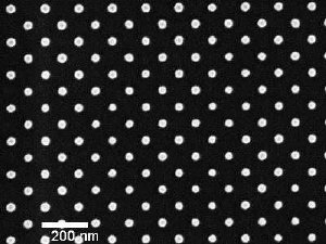
Patterning photonic crystal structures on the surface of LEDs is one of the most promising ways to boost the efficiency. These periodic structures, typically consisting of etched holes at the surface, have periods in the 100-500 nm range. EULITHA has developed a template to be used in high resolution patterning of LED surfaces.
The template, consisting of pillars with a periodicity of 106 nm on a silicon surface, is targeted for use in R&D studies. Areas on the order of several square centimeters are covered by step-and-repeat exposure of 1x1 mm2 dies. The combination of resolution, quality and large areas make these unique templates a perfect choice in the drive to fabricate ever more efficient LEDs.
EULITHA was founded in 2006 in the canton Aargau of Switzerland. Its founders have played critical roles in the development of Extreme Ultraviolet Interference Technology at the Paul Scherrer Institut. The company aims to serve nano-structuring needs of targeted applications through this breakthrough technology. At present, it provides products as samples for nanotechnology R&D.