Engineers and physicists at the University of Pennsylvania have discovered a new chiral property of silicon. They have demonstrated this property in a silicon-based photonic device that is sensitive to the spin of photons in laser light shone onto one of its electrodes.
 By shining lasers with different polarizations on their device, the researchers could make current flow in different directions.
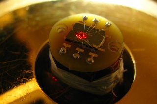
Clockwise polarized light causes current to flow in one direction, while light that is polarized counter-clockwise causes it to flow in the other direction. This property is dependent upon the pattern of atoms on the silicon nanowire surface, and the manner in which the electrodes on the silicon nanowires intersect them. When semiconducting silicon and metallic electrodes interact, an electrical field is produced at such an angle as can break the typically exbited mirror symmetry. This is considered to be the chiral property that causes the electrons to flow in one direction or the other, based upon the polarity of the light that strikes the electrodes.
“Photonic” computers could be many times faster and could demonstrate better efficiency than existing computers when information is encoded in photons through their spin. In a similar manner, when information is encoded in an electron’s spin, it could lead to “spintronic” computers that possess similar advantages.
Ritesh Agarwal, a professor in the Department of Materials Science and Engineering in Penn’s School of Engineering and Applied Science, and Sajal Dhara, a postdoctoral researcher in Agarwal’s lab, have led this study. Eugene Mele, a professor in the Department of Physics and Astronomy in Penn’s School of Arts & Sciences collaborated in this research.
“Whenever you change a symmetry, you can do new things,” said Agarwal. “In this case, we have demonstrated how to make a photodetector sensitive to a photon’s spin. All photonic computers need photodetectors, but they currently only use the quantity of photons to encode information. This sensitivity to photon spin would be an extra degree of freedom, meaning you could encode additional information on each photon."
"Typically, materials with heavy elements show this property due to their spins strongly interacting with electron’s orbital motion, but we have demonstrated this effect on the surface of silicon, originating only from the electron’s orbital motion."
Mele had done work on topological insulators, and this was the reason for the collaboration with Agarwal and Dhara. Mele and Charles Kane, a Penn physicist, had laid the basis for these new types of materials that act as good conductors on the surface and as electrical insulators in their interiors.
When Agarwal’s team had been conducting research on various materials that demonstrated topological effects, Mele proposed that the experiments should also be conducted with silicon.
Silicon is a highly symmetric, light material, and hence it was not believed that it could exhibit the properties.
“We expected the control experiment to give a null result, instead we discovered something new about nanomaterials,” Mele said.
Silicon plays a critical role in the computer industry. Hence, it would be preferable to find out ways to produce topological effects in silicon, rather than in rarer, heavier elements that have these properties.
The group then continued their study to discover the atomic mechanisms behind the ability of silicon to have chiral properties.
“The effect was coming from the surface of the nanowire,” Dhara said. “The way most silicon nanowires are grown, the atoms are bound in zigzag chains that go along the surface, not down into the wire.”
The direction of the zigzag chains did not match exactly with the direction of the electric field, meaning that at some angles, silicon is asymmetric.
This confirmed that silicon could exhibit chiral properties. When a circularly polarized laser is shone on the nanowaire at the specific place where the semiconductor and metal meet, a current is produced. The current’s flow direction is determined by the photons’ spin in the laser.
Agarwal and Dhara are presently conducting research to find out ways to utilize this mechanism to make planar silicon to demonstrate these properties.
This study has been published in Science.
The U.S. Army Research Office, the National Science Foundation and the Department of Energy have supported this study.