Feb 3 2017
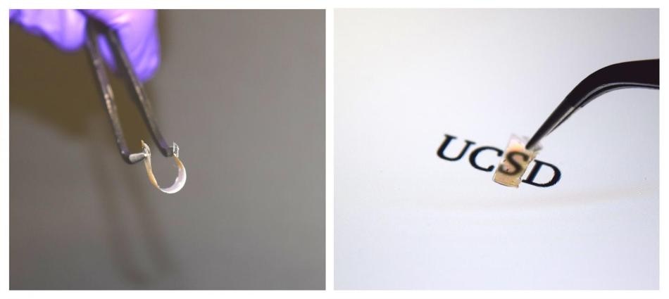
 This is a near-perfect broadband absorber that's thin, flexible and transparent in visible light. (CREDIT - UC San Diego Jacobs School of Engineering)
A team of researchers at the University of California San Diego have developed a thin, flexible, light-absorbing material that has numerous potential applications such as transparent window coatings that keep cars and buildings cool on hot days, devices capable of more than three times the solar cell efficiencies than what is available, and thin, lightweight shields capable of blocking thermal detection.
The material, called a near-perfect broadband absorber, absorbs over 87% of near-infrared light (1,200 - 2,200 nm wavelengths), with 98% absorption at 1,550 nm, which is the wavelength for fiber optic communication. The material can absorb light from all angles. It also can theoretically be tailor-made to absorb specific wavelengths of light while allowing others to pass through.
Materials capable of “perfectly” absorbing light are available now, but they are bulky and can fracture when bent. They also cannot be manipulated to absorb only a specific range of wavelengths, which is a drawback for some applications. It would be like a window coating that is designed for cooling, ended up not only blocking infrared radiation, but also radio waves that transmit radio and TV programs and normal light.
By creating a novel nanoparticle-based design, a team headed by professors Zhaowei Liu and Donald Sirbuly at the UC San Diego Jacobs School of Engineering has developed a broadband absorber that is flexible, thin, and tunable. The research was published online on January 24 in Proceedings of the National Academy of Sciences.
This material offers broadband, yet selective absorption that could be tuned to distinct parts of the electromagnetic spectrum.
Zhaowei Liu, Professor, UC San Diego Jacobs School of Engineering
The absorber relies on optical phenomena called surface plasmon resonances, which are combined movements of free electrons that happen on the surface of metal nanoparticles upon contact with specific light wavelengths. Metal nanoparticles can contain many free electrons, so they display strong surface plasmon resonance - but principally in visible light, and not in the infrared.
UC San Diego engineers explained that if they could alter the amount of free electron carriers, they could tweak the surface plasmon resonance of the material to different wavelengths of light.
Make this number lower, and we can push the plasmon resonance to the infrared. Make the number higher, with more electrons, and we can push the plasmon resonance to the ultraviolet region.
Donald Sirbuly, Professor, UC San Diego Jacobs School of Engineering
The difficulty with this method is that it is difficult to achieve in metals.
To tackle this challenge, the team designed and constructed an absorber from materials that could be doped or, altered, to contain a different number of free electrons: semiconductors. The researchers used zinc oxide, a semiconductor, which has a reasonable amount of free electrons, and merged it with its metallic version, aluminum-doped zinc oxide, which contains a large amount of free electrons — not as much as a real metal, but enough to provide it plasmonic properties in the infrared.
In the Nano3 cleanroom facility at the Qualcomm Institute at UC San Diego, the materials were combined and structured in a specific manner using latest nanofabrication technologies. The materials were placed one atomic layer at a time on a silicon substrate to form an array of vertical nanotubes, each consisting of alternating concentric rings of aluminum-doped zinc oxide and zinc oxide.
The tubes are 650 to 770 nm in diameter, 1,730 nm in height, and spaced less than a 100 nm apart. The nanotube array was later moved from the silicon substrate to a thin, elastic polymer. The end result is a material that is thin, transparent, and flexible in the visible.
“There are different parameters that we can alter in this design to tailor the material’s absorption band: the gap size between tubes, the ratio of the materials, the types of materials, and the electron carrier concentration. Our simulations show that this is possible,” said Conor Riley, a recent nanoengineering Ph.D. graduate from UC San Diego and the first author of this research paper.
Riley is currently a postdoctoral researcher in Sirbuly’s group.
Those are just some of the appealing attributes of this particle-based design, the researchers said. It is also potentially transferrable to all types of substrate and is scalable to create large surface area devices, such as broadband absorbers for big windows.
Nanomaterials normally aren’t fabricated at scales larger than a couple centimeters, so this would be a big step in that direction.
Donald Sirbuly, Professor, UC San Diego Jacobs School of Engineering
The technology however is in the developmental phase. Liu and Sirbuly’s teams will be carrying forward their work together to study various materials, designs, and geometries to create absorbers that function at varied wavelengths of light for a variety of applications.