In an article recently published in the open-access journal Light: Science & Applications, researchers constructed a specific GeSn-on-insulator (GeSnOI) stack with the help of stressor layers as dielectric optical claddings. They also demonstrated that GeSnOI is suitable for monolithic integration of planar Group-IV semiconductor lasers on photonic platforms in the near- and mid-infrared wavelength range.

Study: GeSnOI mid-infrared laser technology. Image Credit: Aumm graphixphoto/Shutterstock.com
Why Use GeSn Alloys in Mid-Infrared Lasers?
Cost-effective, CMOS-compatible Si-based photonic technologies such as silicon-on-insulator (SOI) have enabled advanced on-chip optical processing in the near-infrared range, particularly in high-speed detection and optical signals modulation. However, the lack of monolithically integrated Group-IV lasers is a major drawback.
For decades, researchers have been working on the integration of III–V compounds with high lasing performances to improve silicon photonic technologies. Despite high manufacturing costs and complex integration in Si CMOS-compatible manufacturing, III–V lasers are the most reliable light sources on silicon so far.
GeSn semiconductor alloys have a direct bandgap for tin contents larger than 7% and are compatible with low-cost and large-scale silicon processing and manufacturing tools, making them ideal for use in low-cost lasers.
Additionally, compared to Ge, GeSn alloys have a narrow bandgap and thus can shift the photonic wavelength from near-IR to mid-IR, which is ideal for a wide range of applications including gas monitoring, biochemical detection, and thermal imaging. The integration of GeSn on silicon paves way for new applications in Si photonics.
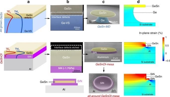
Design and fabrication of GeSnOI planar cavities. a Schematic diagram of as-grown GeSn on Ge SRB and GeSnOI stacks together with TE and TM mode profiles of a confined optical wave at a 2.4 µm wavelength. More details are given in the SI (Fig. S3). b X-TEM images of as-grown GeSn on Ge SRB and of GeSnOI stacks. c Scanning electron microscopy (SEM) images of GeSn and GeSnOI and all-around strained microdisk cavities. A cross-sectional schematic representation of the GeSnOI mesa fully cladded with SiN can be found on the left of the bottom SEM image (d) in-plane strain variation, analyzed by Finite Element modeling (FEM), of GeSn and GeSnOI microdisks with 7 µm diameters that due to the different designs and processing adopted. Here we plot the strain relative to initial residual post-growth compressive strain of −0.5% for the GeSn layer. The SiN layer was computed with initial compressive stress that can relax, thus inducing positive strain variation. Image Credit: Wang, B et al., Light Science Applications
About the Study
The researchers bonded a Ge0.9Sn0.1 alloy layer grown on a Ge strain-relaxed-buffer on a Si(001) substrate and fabricated microdisk-shape resonators on mesa structures. The as-grown layers were analyzed using X-ray diffraction reciprocal space mapping and the layers had a residual compressive strain of −0.5%. The authors also performed whispering gallery mode (WGM) analysis and their scattering by the Al grating as per the aperiodic Fourier modal method.
After bonding the GeSn layer, the dense array of misfit dislocations near the GeSn/Ge interface was eliminated using a simple etching step, resulting in improved quality of active layer which in turn improves carrier injection efficiency. These bonded structures also open up the possibility of having the GeSn layer on top of an aluminum layer, which helps with better heat dissipation.
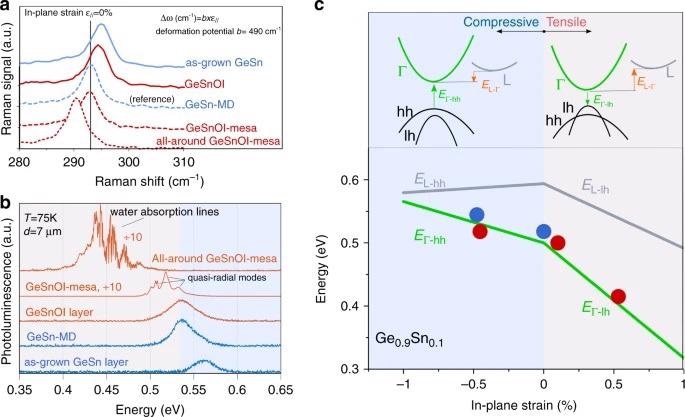
Optical analysis of strain. a Raman spectra of LO-phonon vibrations in the blanket, as-grown GeSn 10.5% on Ge SRB stacks, blanket GeSnOI stacks, GeSn-on-Ge SRB microdisks, GeSnOI mesas, and all-around GeSnOI mesas. The diameter of disks and mesa was 7 µm. b Photoluminescence spectra of GeSn layers as in (a) excited with cw optical pumping. c Direct and indirect bandgap energies of GeSn as a function of strain. Direct bandgap energies from PL measurements appear as blue circles for the as-grown GeSn 10.5% on Ge SRB stack and the GeSn-on-Ge SRB microdisks. Red circles show the PL energies for the blanket GeSnOI stack, the GeSnOI mesa, and the all-around GeSnOI mesa (from left to right). Full lines are calculated direct bandgap (green) and indirect bandgap (gray) energies as functions of strain using model as described in ref. The top picture is a schematic scenario of band structure for compressive and tensile-strained GeSn. Image Credit: Wang, B et al., Light Science Applications
Observations
The GeSnOI microdisk mesas showed a significantly higher optical gain compared to conventional suspended microdisk resonators produced from the as-grown layer. They further exhibited improved vertical out-coupling of the disk WGM in-plane radiation, with nearly 30% vertical out-coupling efficiency.
This work shows that GeSnOI stacks produced through the bonding of GeSn active layers resolve all major limitations discussed above such as compressive/tensile strain management, lattice mismatch interface defects management, and optical confinement.
The team demonstrated these by systematically comparing the two structures with equivalent optical confinements - a suspended microdisk cavity produced from a GeSn layer on a Ge SRB and another cavity fabricated using the GeSnOI method, with specific SiN stressor films acting as insulating layers and a simple disk-shape mesa serving as the cavity.
The SiN layers used for tensile strain engineering provided high index contrast with GeSn, which is needed for optical confinement. Disk cavities bonded to the substrate without any under-etching made it possible to downscale their diameters to 3 µm, which was not possible with as-grown GeSn-microdisk. The lowest achievable diameters of as-grown GeSn-microdisk without affecting mechanical and thermal robustness was 5 µm.
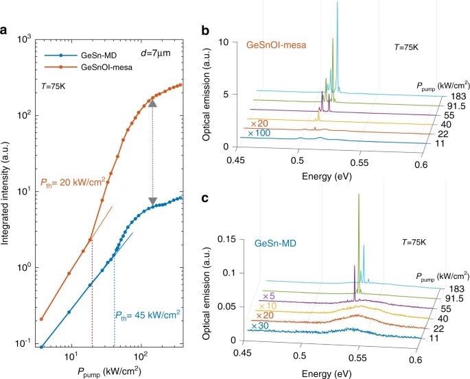
GeSnOI mesa versus as-grown GeSn microdisk laser. a Light–Light (L–L) curves of 7 µm diameter GeSn microdisks and GeSnOI mesas with 360-nm-thick GeSn at 75 K under pulsed pumping (b) and c PL spectra at 75 K for various pulsed excitation powers for the GeSnOI mesa and the GeSn-MD, respectively. Excitation levels are given by the peak power densities. Image Credit: Wang, B et al., Light Science Applications
Conclusions
To summarize, the microdisk-shaped mesas etched in bonded GeSnOI stacks had many advantages compared to suspended GeSn microdisks. A GeSnOI disk-shape mesa had no interfacial defects that were seen in the suspended GeSn-microdisk at the pedestal’s GeSn/Ge interface.
The bonded structure in GeSnOI disk-shape mesa is not under-etched and has an aluminum layer that acts as a heat sink leading to better thermal management.
The optical confinement of optical modes in the active GeSn layer is equally good in GeSnOI mesas compared to under-etched structures suspended in the air. Additionally, a full cladding of the GeSn mesa with SiN insulator layers offers high levels of homogeneously distributed tensile strain, which is not feasible with a suspended GeSn-microdisk.
The main advantage of this GeSnOI platform is its ability to blend active laser structures with passive SiN circuitry from the near-infrared range to the mid-infrared range.
This represents a new standard for infrared Group-IV photonics that removed the need for III–V laser integration. Thus, the GeSnOI approach is a valuable resource in the development of silicon-based mid-infrared photonics that combines complex lightwave engineering with integrated sources in a photonic platform.
Source
Wang, B., Sakat, E., Herth, E. et al. GeSnOI mid-infrared laser technology. Light Sci Appl 10, 232 (2021). https://www.nature.com/articles/s41377-021-00675-7
Disclaimer: The views expressed here are those of the author expressed in their private capacity and do not necessarily represent the views of AZoM.com Limited T/A AZoNetwork the owner and operator of this website. This disclaimer forms part of the Terms and conditions of use of this website.