Perovskite-based solar cells, often seen as the next-generation successors to the currently predominant silicon cells, are gaining substantial attention due to their streamlined and cost-effective manufacturing process, coupled with their exceptional performance.
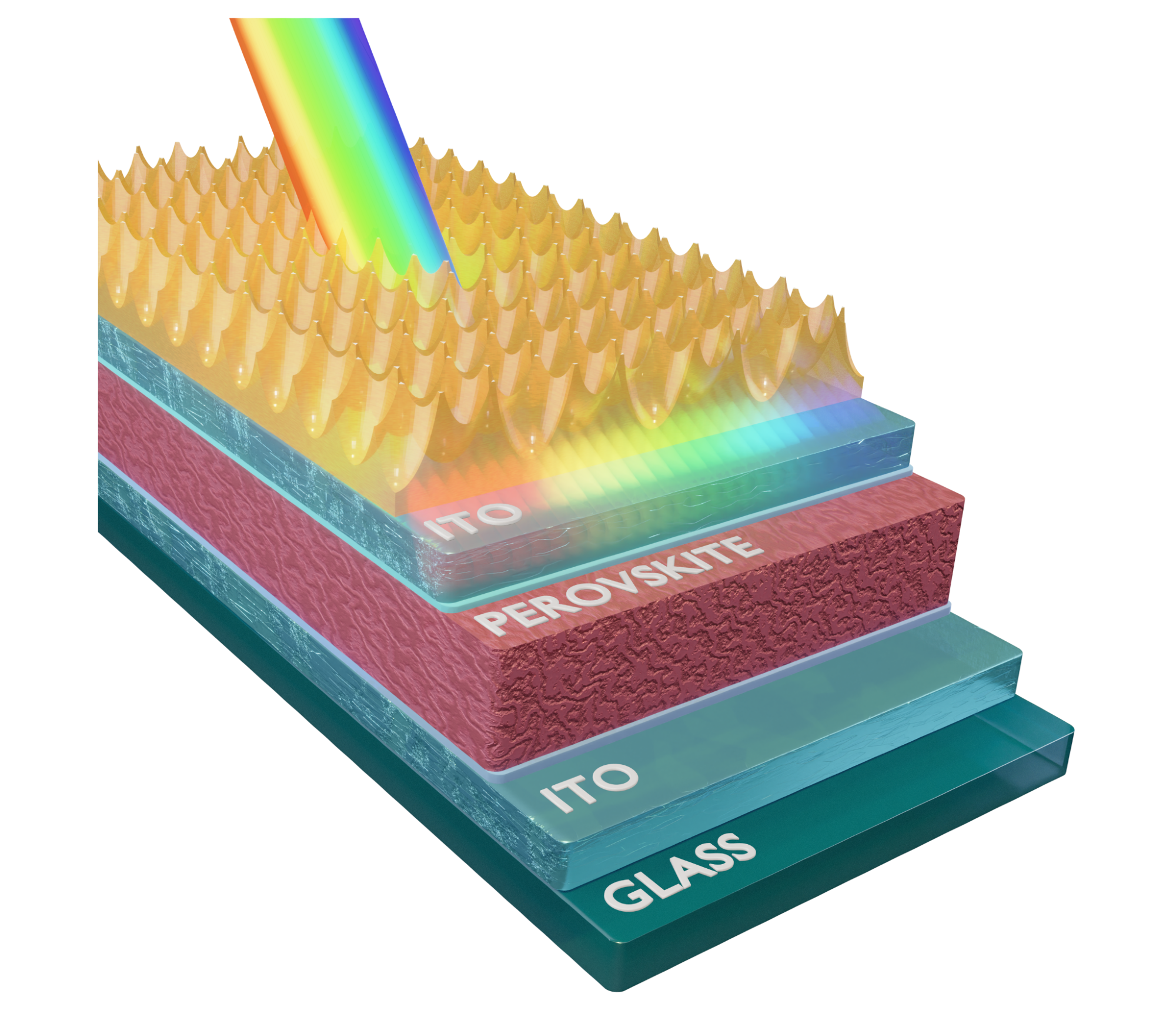 The visualization of the manufactured honeycomb texture for the perovskite solar cell. The research of the team of scientists was appreciated by being presented on the cover of the journal Advanced Materials and Interfaces. Image Credit: Maciej Krajewski, Faculty of Physics at the University of Warsaw.
These solar cells are currently undergoing comprehensive research. In a recent publication in the journal Advanced Materials and Interfaces, a team of scientists from the Fraunhofer Institute for Solar Energy ISE and the Faculty of Physics at the University of Warsaw unveiled perovskite photovoltaic cells featuring significantly enhanced optoelectronic characteristics.
The reduction of optical losses, as demonstrated in the paper, stands as one of the pivotal challenges in expanding the use of these next-generation cells.
The field of photovoltaics has witnessed remarkable progress in the last two decades, marked by advancements in both panel efficiency and installed capacity. Since the year 2000, global installed capacity has skyrocketed, increasing by a staggering factor of 1000.
While silicon has been the predominant material for manufacturing photovoltaic panels, cells based on silicon are nearing their physical efficiency limits. Consequently, researchers are actively engaged in exploring innovative solutions aimed at improving cell efficiency while enabling more cost-effective and environmentally friendly production methods.
Perovskite-based cells meet both criteria, offering efficiency above 26%, ease, and cost-effectiveness in production using well-established chemical methods. Currently, numerous research institutes worldwide are working on improving their efficiency and resistance to atmospheric conditions.
One of the challenges they face is the integration of perovskite cells with silicon cells while simultaneously reducing losses from reflection and parasitic absorption. To minimize these losses, silicon cells are typically etched with highly corrosive chemical agents, a process that creates a microscopic pyramid pattern on the surface, effectively reducing the reflection of the entire device, and thereby increasing the current generated by the device.
Unfortunately, perovskites are sensitive to many chemical substances, so less effective planar anti-reflective coatings applied through less invasive sputtering have been employed.
Researchers employed the nanoimprinting technique to create an efficient anti-reflective structure with a honeycomb-like pattern on the surface of perovskite solar cells. This innovative method enables the fabrication of nanoscale structures across extensive surfaces, surpassing 100 cm² in size.
This approach guarantees scalability in the production process of large-surface devices, which is crucial in the context of the urgent need for energy transformation toward renewable energy sources.
Msc Maciej Krajewski, Researcher, Faculty of Physics, University of Warsaw
These modified samples exhibited enhanced efficiency compared to cells using conventional planar anti-reflective layers.
In addition to its efficiency improvements, another noteworthy discovery from the published research is that the application process for this layer does not harm the perovskite material. This breakthrough paves the way for exploring alternative structures customized to specific cell architectures. Up until now, scientists had been applying similar anti-reflective structures as distinct layers, which required a separate manufacturing process. This process was inherently limited in scale and posed a risk of damaging the active layer.
By embracing the direct nanoimprinting method, it becomes feasible to fabricate the entire device on a large scale and within a single technological process. This advancement holds significant importance in the quest to reduce the overall costs associated with these devices.
Moreover, the employed method is conducive to a tandem configuration, wherein silicon and perovskite cells are combined. This compatibility introduces entirely new possibilities for its utilization.
As a result, there is the prospect of directly applying this procedure to emerging photovoltaic architectures, which could yield further enhancements in efficiency. The findings published in the research paper lay the foundation for the development of novel photovoltaic devices boasting exceptional optoelectronic characteristics, with nanoimprinting techniques playing a pivotal role in their production.
The experiment and modeling were conducted at Fraunhofer ISE in Freiburg, with the participation of researcher Msc. Maciej Krajewski from the University of Warsaw. Funding for the research was provided by: Fraunhofer Gesellschaft (project MEEt within the ICON program), the Institute of Experimental Physics at the Faculty of Physics UW, University of Warsaw, Faculty of Physics UW, University of Warsaw Foundation, as well as from the Erasmus+ program and the Deutsche Bundesstiftung Umwelt.
Journal Reference:
Krajewski, M., et al. (2023). Roller Nanoimprinted Honeycomb Texture as an Efficient Antireflective Coating for Perovskite Solar Cells. Advanced Materials Interfaces. doi.org/10.1002/admi.202370076.
Source: https://en.uw.edu.pl/