A standard step utilized for sample characterization is to outline the microstructure and detect areas of interest for additional analysis. On a scanning electron microscope (SEM), this usually means using backscatter electron (BSE) or secondary electron (SE) detectors to produce images.
However, when working with samples in slanted geometry, the BSE detector cannot be used all the time, while the SE detector is not always in the suitable geometry. Thus, the signal for both these detectors may be compromised. In order to improve imaging at this geometry, EBSD detectors have Forescatter diodes (FSD) that are attached below and above the phosphor screen.
Forescatter Diodes
FSD diodes can be utilized for imaging purposes, and thanks to their position around the EBSD detector, they are capable of detecting electrons that interact with the sample in numerous ways. This results in different images and different contrast mechanisms, as shown in Figure 1.
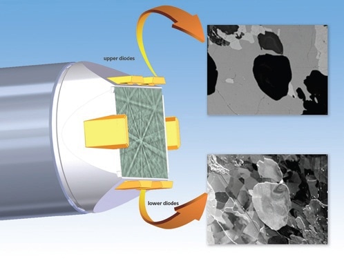
Figure 1. The positioning of the forescatter diodes and examples of the images collected from a geological sample by the upper and lower diodes.
The lower diodes mainly detect electrons that have undergone a low-angle scattering, emitting from the interaction with the lattice and resulting in images produced based on orientation contrast. The upper diodes detect BSE (large-angle scattering) and reveal differences in chemistry.
PhaseID
For an EBSD system to index an EBSP, it must know which phase(s) to index against. Hence, the initial step of the investigation is to detect the phases that exist in the sample. In case the EBSD system is not combined with an EDS system, the user should know in advance what phases are there in the sample, either from the sample history or from EDS analysis undertaken separately.
Based on this knowledge, users can create a list of potential phases. On the other hand, the list may include phases that are not in the sample. In order to confirm which phases exist, the FSD image serves as a valuable reference for obtaining reference EBSPs from numerous regions and tracking those EBSPs against the list of phases that are produced manually.
If both the EDS and EBSD systems are combined and mounted in an appropriate geometry on the SEM, the FSD image can be used as a reference, and the beam can be placed on each potential phase to achieve an EDS spectrum and an EBSP simultaneously.
For each position of the beam, the system looks for available crystal structure databases for entries that correspond to the phase chemistry. These phases can be utilized for indexing the collected EBSP, and the system locates the structure based on crystallographic and chemical data.
Also, chemical element maps can be used as a reference, but it is better to utilize the FSD images as they include data regarding the grain structure, thus making it possible to detect small-sized particles and ensuring that the beam is positioned not on a boundary, but within a grain.
Phase Discrimination
The Kikuchi pattern that is detected is produced by the beam of electrons that interact with the crystal structure in the sample’s surface. By studying the EBSP, data can be obtained about the crystal’s orientation and information can also be obtained which helps in differentiating between different crystal structures and phases. An example is illustrated in Figure 2.
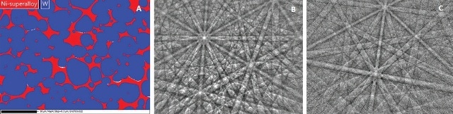
Figure 2. The discrimination of the two phases present in a sample of tungsten hardened alloy. A) A phase map showing the two separate phases (Ni is shown in red and W in blue). B) A typical EBSP obtained for W. C ) A typical EBSP for Ni.
EBSPs are normally studied by viewing the angles between the detected bands. If this data alone is utilized, it is possible to differentiate between phases having different unit cell structures, provided a single structure is not a mere scaling of another (Figure 3).
Present-day systems are capable of collecting data regarding the band width within the EBSPs and thus help in differentiating between phases of the same type of structure but different lattice parameters.
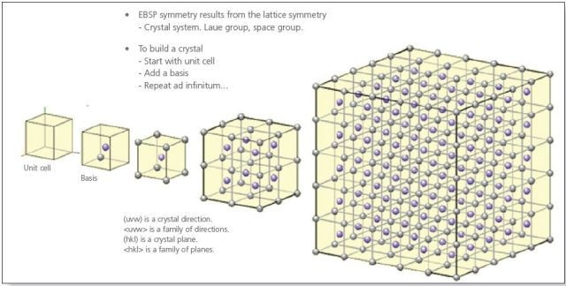
Figure 3. The scaling of unit cell structures.
Point Analysis
Point analysis is essential to track whether the EBSPs are of a reasonable quality prior to collecting information from a sample such as maps. In case the EBSPs appear reasonable, it is important to check the band detection settings and whether the EBSP can be effectively indexed depending on the phases in the phase list.
When these steps are repeated at different beam positions, users can get an overview of the microstructure. Figure 4 shows an example where point analysis is utilized to obtain information and establish the orientation in some selected grains.
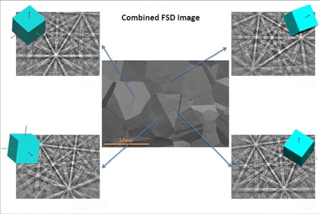
Figure 4. Point analysis of grains in steel showing the diffraction pattern generated and the calculated crystal orientation in Euler Angles.
Mapping
The standard sequence for manual point analysis is as follows:
- Position beam
- Acquire EBSP
- Detect bands
- Index based on phase list
- Save the result
At each beam position, the system saves pattern quality values measured based on the EBSP; Euler angles; phase data; mean angular deviation; orientation; and EDS information if the EDS and EBSD systems are combined together. Once all the parameters have been setup, this flow can be automated to extend a large sample area.
Typical Data Presentations
PhaseMap
Different map displays can be created based on the saved data, for instance, a map can created that shows how the phases are dispersed within the sample. This is achieved by assigning a colour to each phase and colouring the map pixel depending on which phase was identified during the analysis, (Figure 2).
Pattern Quality Map
Pattern quality values are measured based on the peak profile or peak intensity in the Hough space. One way to determine a pattern quality parameter p would be:
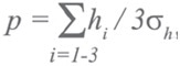
where σh is the standard deviation of the Hough transform and hi is the peak height of the Hough transform of the i’th most intense Kikuchi band. However, pattern quality values are determined in a more sophisticated manner.
The pattern quality parameter will associate a number with how well defined the band positions are in the EBSP. In other words, the pattern quality (Figure 5) will be influenced by a number of factors such as orientation, phases, sample preparation, contamination, and the local crystalline perfection.
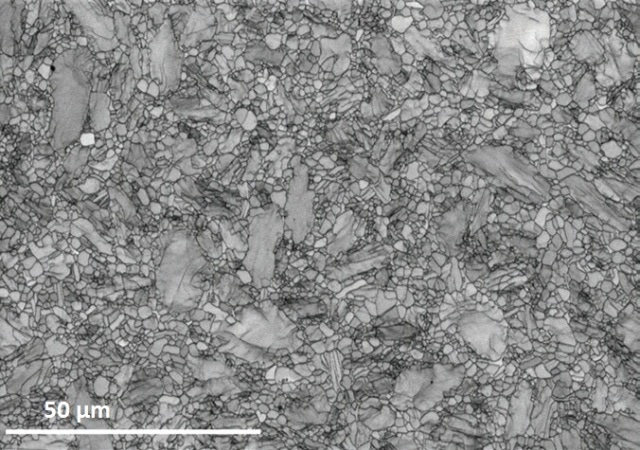
Figure 5. A pattern quality map for a sample of Ti64. Dark areas are indicative of poorer pattern quality and light areas of higher pattern quality.
Pattern quality maps show features that cannot be seen in the electron image such as grains, internal grain structure, grain boundaries, and scratches, thus making the pattern quality map quite useful during data analysis. Such maps are simple tools that can be used for tracking whether the sample remained in focus during data collection or drifted.
Conclusion
EBSD has become a proven accessory for the SEM, which is utilized to provide crystallographic data routinely. EBSD data, when utilized in tandem with a data base that comprises crystallographic structure data for phases of interest, can be utilized to detect phases based on the crystal structure and also to perform fabric analyses on polycrystalline aggregates.

This information has been sourced, reviewed and adapted from materials provided by Oxford Instruments NanoAnalysis.
For more information on this source, please visit Oxford Instruments NanoAnalysis.