EVG’s pioneering technological advancements have defined industry standards in both top and double-sided lithography, aligned wafer bonding and nanoimprint lithography. The company has been at the cutting edge of this field since it developed the world’s first bottom-side alignment system in 1985.
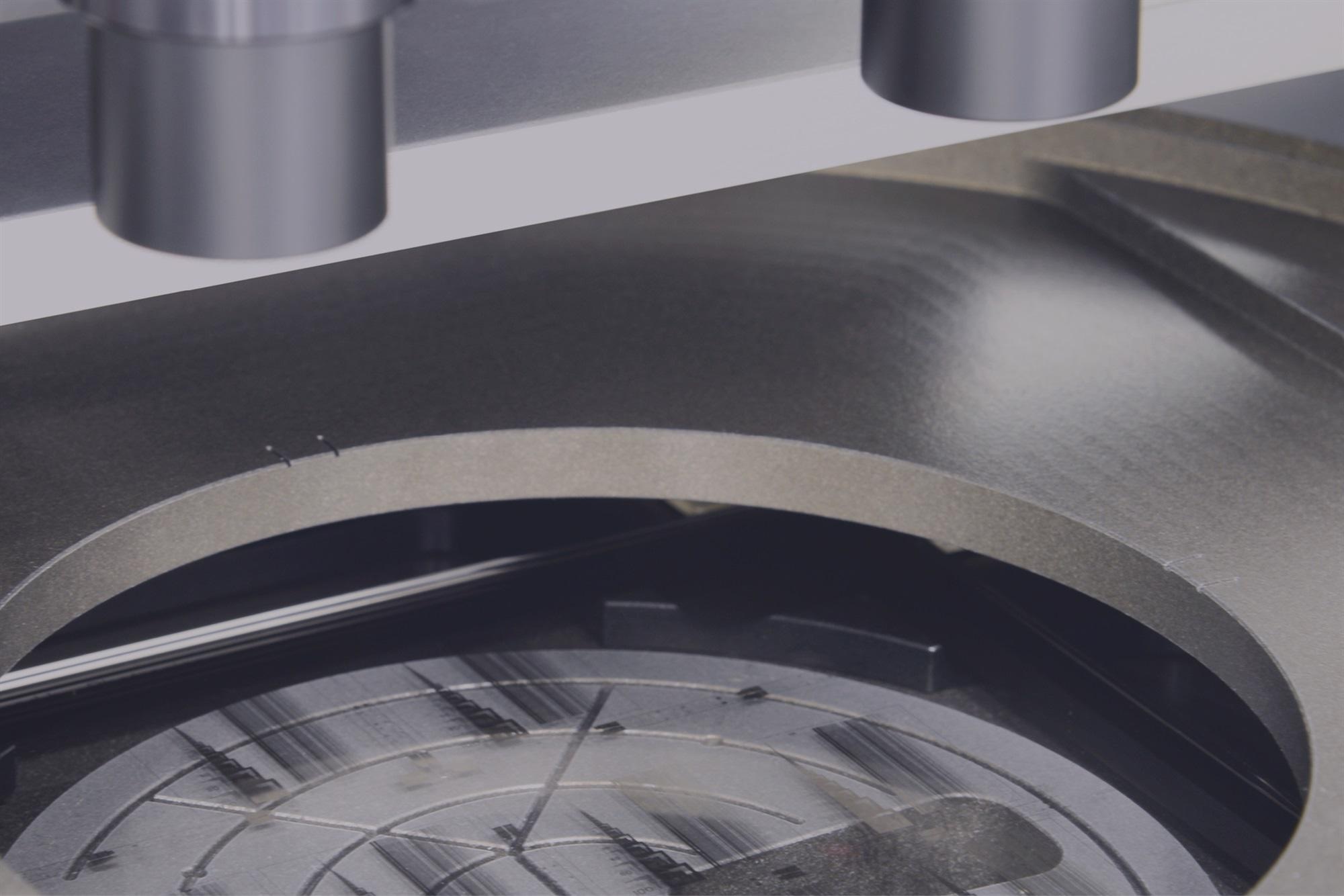
Image Credit: EV Group
EV Group continuously develops new generations of mask aligners able to augment even the most ground-breaking lithography technology. EV Group’s mask alignment solutions can accommodate wafers and substrates up to 300 mm, regardless of their size, shape and thickness. The company’s goal is to provide sophisticated high-tech solutions for advanced applications while simultaneously offering the maximum flexibility required for ongoing research and development.
EVG’s mask aligners and process competence are installed and thoroughly integrated in the worldwide network. These devices can be found in a wide range of applications; for example, advanced packaging, power devices, compound semiconductors, LED components, MEMS and sensors.
EVG is consistently monitoring and anticipating future market trends (for example, photonics and optical 3D sensing), routinely developing and adapting its solutions to meet its customers’ ever-evolving requirements.
This ethos has seen EVG maintain continued technological and market leadership, with the company’s unparalleled experience allow it to employ a range of non-standard resists optimized to accommodate specific parameters and requirements. Thoroughly comprehending customer needs and meeting these via efficient worldwide support are also key elements of EVG’s solutions and approach.
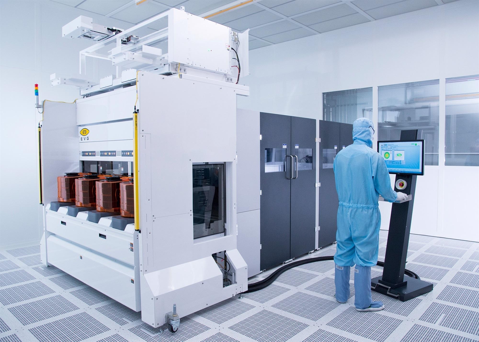
Image Credit: EV Group
State-of-the-Art Engineering
Key requirements for proximity aligners are currently defined as sub-micron alignment accuracy, a controlled and uniform proximity gap between wafer and mask, and an easily controlled, clearly defined exposure spectrum that corresponds to resist sensitivity. It is also important to ensure high light intensity and uniformity across the full wafer surface.
These are just some of a significant number of crucial parameters taken into account as EVG continues to design, develop and continuously enhance its mask aligner product portfolio. The company is driven by innovation and its ability to think outside the box.
Optimized Multi-Purpose Systems
EVG’s mask alignment systems have been designed to facilitate quick and easy conversion from mask alignment to bond alignment. Optional toolsets are available for imprint lithography; for example, UV-nanoimprint lithography, microcontact printing or hot embossing. All of the company’s systems can work with in-situ alignment verification software, enabling increased alignment accuracy and repeatable performance on systems that are manually operated.
The EVG620 NT / EVG6200 NT can be field-upgraded from manual to automated substrate handling, and EVG’s proprietary NIL technology can be employed in all of the company’s mask aligners.
Research and Development
EVG has over 35 years of experience in working with research facilities, affording the company considerable insight into their often unique requirements. EVG’s dedicated R&D tools offer a combination of superior technology and maximum flexibility, ideal for research institutions, universities and technology development partners looking to scale processes across a number of applications and research projects.
R&D equipment can be integrated seamlessly into EVG’s core technology platforms. These platforms span the whole manufacturing chain, ranging from initial R&D to small-scale and high-volume production. Software and recipe compatibility is maintained between R&D and full-scale production systems, ensuring that researchers can easily migrate processes to volume-production environments.
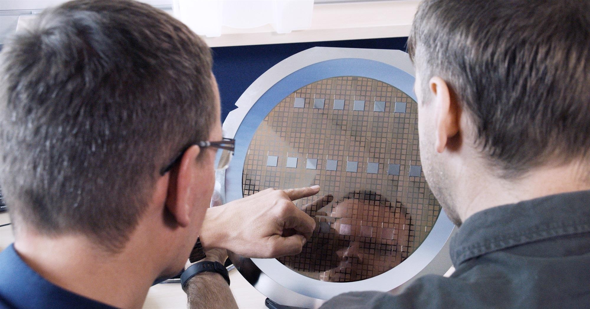
Image Credit: EV Group
High-Volume Mask Alignment Systems
Mask aligners remain the most cost effective solution for lithographic patterning in the single micrometer range, typically offering cost savings of more than 30% per layer when compared against other solutions.
EVG’s high-volume manufacturing systems have been designed to ensure the highest technological standards coupled with optimal cost efficiency. These systems are also supported by a first class, worldwide service infrastructure.
Large depth-of-focus exposure optics are ideal solutions for patterning thick resists, topography, and non-flat substrates in high-volume production applications.
EVG®610 Mask Alignment System
- Stand-alone system, that can accommodate wafer sizes up to 100 mm, 150 mm and 200 mm
- Top-side / bottom-side alignment as low as ±0.5 µm / ±2.0 µm
- High-resolution top- and bottom-side split field microscopes, ideal for double-side alignment
- Soft-, hard-, vacuum-contact and proximity exposure
- Bond Alignment and NIL option
- Automated wedge compensation
- Support for current UV-LED technology
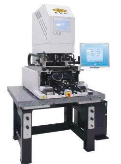
Image Credit: EV Group
EVG®620 NT / EVG®6200 NT
- Semi-automated / automated mask alignment system
- Production system able to accommodate wafer sizes up to 150 mm and 200 mm
- Proximity wedge error compensation
- Able to accommodate multiple wafer sizes with rapid changeover time of under 5 minutes
- Up to 140 wph automatic alignment mode
- Up to 180 wph first print mode
- Optional stand-alone version complete with anti-vibration granite table
- Dynamic alignment function including real-time offset correction
- Support for current UV-LED technology
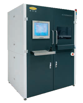
Image Credit: EV Group
IQ Aligner®
- Able to accommodate wafer sizes up to 200 mm
- Up to 80 wph automatic alignment mode
- Up to 90 wph first print mode
- Top-side / bottom-side alignment as low as ±0.5 µm / ±1.0 µm
- Proximity processing capability - 100% contactless
- Ergoload cassettes with options for SMIF or FOUP
- Precise run-out compensation ensures optimum overlay alignment
- Able to accommodate manual substrate loading
- Transmissive and/or reflective IR alignment capability
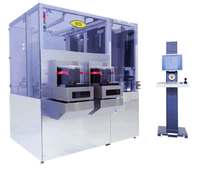
Image Credit: EV Group
IQ Aligner® NT
- Zero assist bridge tool - a dual substrate concept that enables flexibility of production for 200 mm and 300 mm wafers
- Unmatched throughput (first print / aligned) up to 140 wph
- Top-side / bottom-side alignment as low as ±250 nm / ±500 nm
- Proximity processing capability - 100% contactless
- Darkfield alignment capabilities with full clearfield mask movement (FCMM)
- Precise run-out compensation ensures optimum overlay alignment
- Performance analysis framework software
- Smart process control
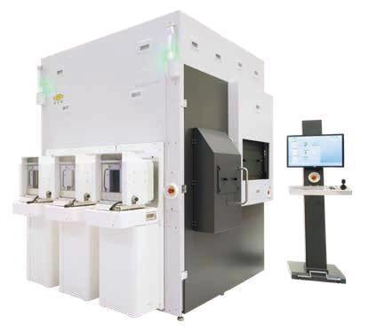
Image Credit: EV Group
HERCULES®
- Fully automated lithography track system
- Modular design
- Ideal for mask alignment and exposure
- Integrated pre- and post-processing
- High throughput wafer processing
- Up to 8 wet-processing modules along with up to 24 extra bake, chill and vapor prime plates
- Mask alignment and exposure can employ EVG’s IQ Aligner® or EVG®6200 NT technology
- Separate cabinet for chemistry handling
- Supports Continuous Mode of Operation (CMO)
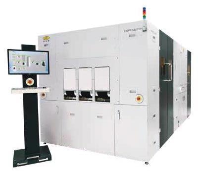
Image Credit: EV Group
Manual and Automated Handling
EVG’s automated systems can also accommodate manual substrate loading. Manual mask loading is also possible - ideal for detailed process evaluation. It is possible to configure the systems to work with bowed, warped, thinned or non-SEMI-standard-shaped substrates and wafers. A range of wafer chuck designs is available, ensuring the highest level of process flexibility and uncompromised substrate handling.
The company’s mask aligners can also be fitted with mechanical or non-contact optical pre-aligners, with the Load & Go option ensuring that automated systems can start processes extremely quickly.
Alignment Enhancements
The use of fully motorized top- and bottom-side split field microscopes helps to facilitate efficient live, large gap, wafer flat or IR alignment. These microscopes are also able to be automatically placed according to pre-programmed positions.
Recipe-controlled, optimal pattern contrast is assured for both brightfield and darkfield illumination with advanced pattern recognition algorithms, auto-origin functionality, synthetic alignment key pattern import and training, ensuring that alignment results are highly reproducible.
Exposure Optics
An array of exposure optic configurations are available, designed to ensure that almost any application can be adapted to. Mercury arc lamp exposure optics are optimized for use with 150 mm, 200 mm and 300 mm substrates. These can also be utilized with specific filters to meet narrow-band exposure requirements; for example, i-, g-, and h-line filters or deep ultra-violet.
Resolution Enhanced Optics (REO) deliver 50% higher intensity and markedly improved resolution, reaching feature sizes of less than 3 µm when used in proximity mode. REO’s specialized design can utilize controlled interference effects in order to increase resolution.
EVG has recently begun offering an LED lamp setup that can further enhance exposure optics. This technology offers low energy consumption and a long lifetime, because UV-LED light sources do not require a warm-up or cool-down phase. A user-friendly software interface enables straightforward, practical exposure spectrum setup.
LEDs only require power during exposure, and this innovative technology effectively eliminates the need for additional facilities such as exhaust or cooling gases. Frequent lamp changes common with mercury arc lamps are also no longer necessary.
The use of UV-LED light sources offers an ideal combination of minimal running and maintenance costs, enhanced operator safety and improved environmental friendliness.
Image Credit: EV Group
Software and Support
A user-friendly Windows-based, graphical user interface is available. This system has been designed with a strong focus on usability, efficiently guiding the operator through each process step in a streamlined manner. Multi-language support is available, while accountability and simple daily operation is ensured via individual user account settings and integrated error logging, reporting and recovery.
EVG systems are all capable of remote communication, meaning that real-time remote diagnostics and troubleshooting are always available via phone, e-mail or secured remote connection. EVG’s experienced process engineers are on hand at any time thanks to the company’s decentralized worldwide support structure, which features cleanroom space across three different continents: Europe (HQ), North America (USA) and Asia (Japan).
Image Credit: EV Group
Summary
EVG’s experience and expertise in lithographic technology have been fundamental in ensuring the advanced high-throughput proximity and contact exposure capabilities of its range of mask alignment systems (the EVG6xx and IQ Aligner series) and in its series of highly integrated coating platforms (the EVG1xx series).
EVG’s full range of lithography equipment platforms are 300 mm ready, and these can be fully integrated into the company’s HERCULES lithography track systems. The company’s full range of systems is also complemented by its array of metrology tools designed for top-to-bottom side alignment verification.
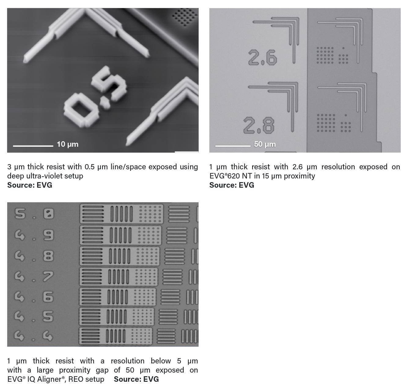
Image Credit: EV Group
Advanced Packaging
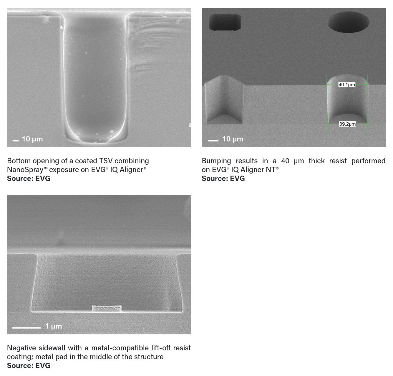
Image Credit: EV Group
MEMS
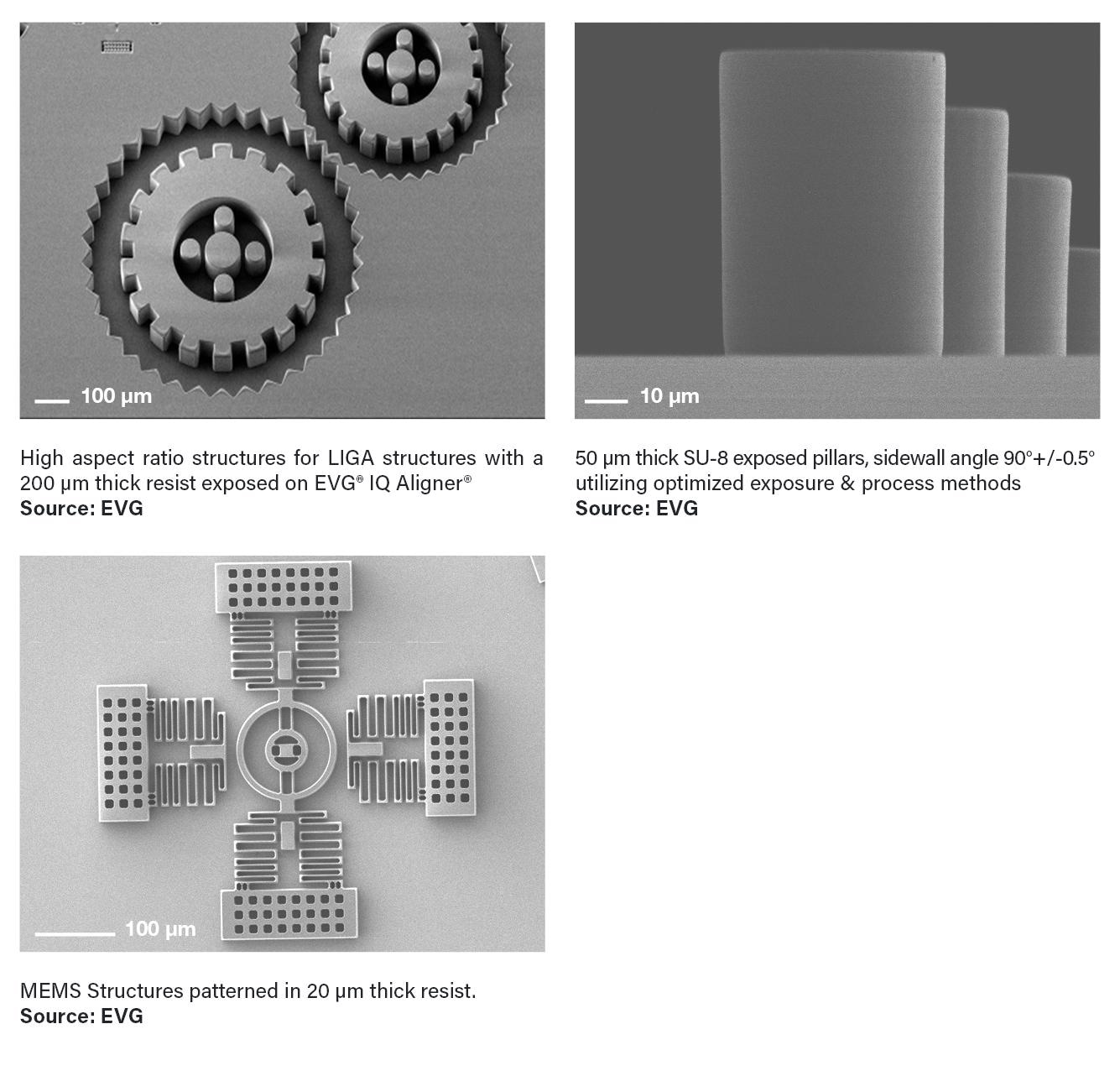 Image Credit: EV Group
Photonics, Special Applications
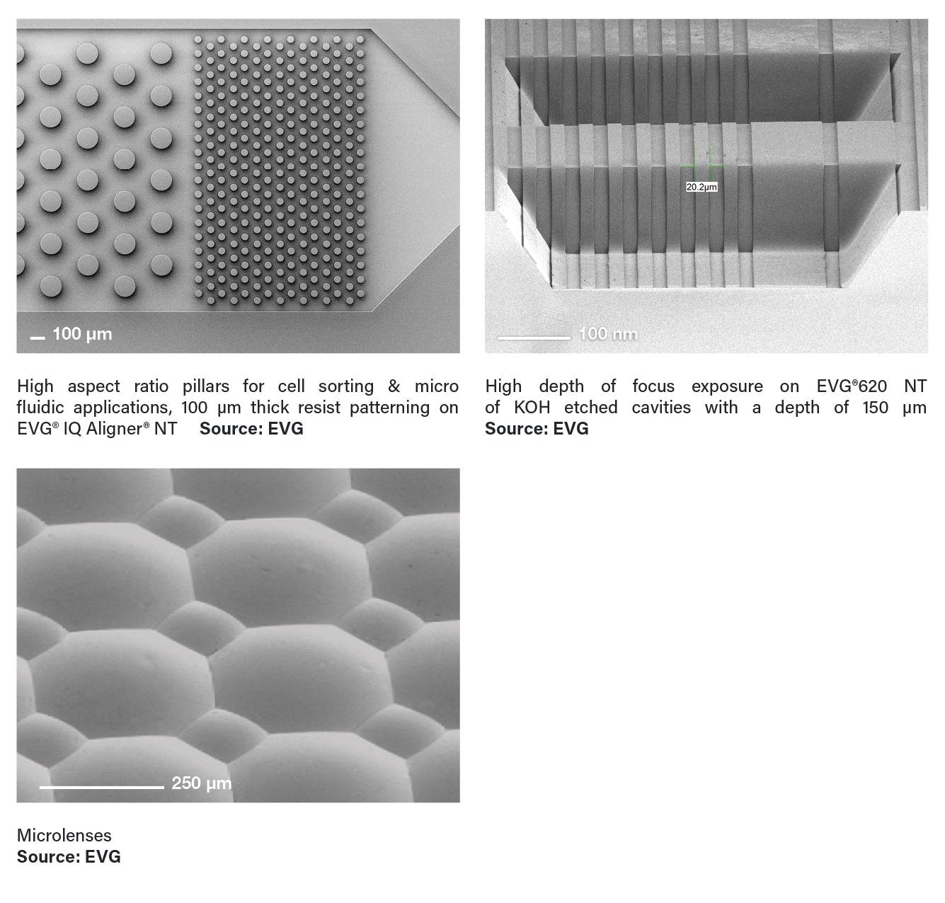
Image Credit: EV Group
About EV Group
EV Group (EVG) is a leading supplier of high-volume production equipment and process solutions for the manufacture of semiconductors, MEMS, compound semiconductors, power devices and nanotechnology devices.
A recognized market and technology leader in wafer-level bonding and lithography for advanced packaging and nanotechnology, EVG’s key products include wafer bonding, thin-wafer processing and lithography/nanoimprint lithography (NIL) equipment, photoresist coaters, as well as cleaning and inspection/metrology systems.
With state-of-the-art application labs and cleanrooms at its headquarters in Austria, as well as in the U.S. and Japan, EVG is focused on delivering superior process expertise to its global R&D and production customer and partner base – from the initial development through to the final integration at the customer’s site.
Founded in 1980, EVG services and supports an elaborate network of global customers and partners all over the world, with more than 1000 employees worldwide and fully-owned subsidiaries in the U.S., Japan, South Korea, China and Taiwan.
This information has been sourced, reviewed and adapted from materials provided by EV Group.
For more information on this source, please visit EV Group.