Ever-changing demands on electronic device flexibility and performance are shifting manufacturing infrastructure away from conventional mask-based lithography, increasingly employing digital lithography solutions for heterogeneous integration and advanced packaging.

Image Credit: EV Group
Systems on chip are no longer reliant on monolithic solutions, rather, these are increasingly employing modular systems in package, chiplets and functional blocks.
There is a growing demand for scalable, versatile back-end lithography to facilitate interconnection on both the package and system level. To meet this new industry vision, there is a need for new tools for mass production that can swiftly integrate novel functional elements via advanced packaging. Therefore, the high-volume- manufacturing (HVM) industry must look beyond conservative chip patterning to fully embrace this new era of digital lithography technology.
EV Group has developed the MLE™ (Maskless Exposure) technology, effectively eliminating mask-related difficulties and costs to better provide design flexibility and minimal development cycle requirements in the HVM sector. MLE™ resolves the disruption between versatile (but time-consuming) development machinery and rapid (but inflexible) production methods.
MLE™ is a scalable solution that enables die- and wafer-level design simultaneously while supporting new and established materials and delivering high-speed adaptability. It offers these benefits along with high reliability and multi-level redundancy, ultimately resulting in lower cost of ownership (CoO) and greater yield.
EVG’s MLE™ technology meets critical back-end lithography requirements in advanced packaging, biomedicine, MEMS, and printed circuit board manufacturing.
The MLE™ technology offers a number of key benefits:
- Full-resolution, stitch-free dynamic photoresist patterning
- Better than 2 µm line / space resolution in any direction
- Design freedom and data confidentiality is ensured by digital programmable layouts
- Individual die annotations are available; for example, encryption keys and serial numbers
- Compensation of wafer-level adaptive registration
- Not impacted by substrate warpage and deformation such as glass, thick wafers, or organic substrates
- An agile and smart digital lithography processing infrastructure
- Does not require consumables
Heterogeneous integration is a fast becoming a central driving force in semiconductor development and innovation. This is increasingly impacting the advanced packaging, MEMS and PCB markets, resulting in growing requirements for back-end lithography.
In advanced packaging applications, minimum resolution requirements for redistribution layers (RDL) are becoming increasingly stringent. This is also the case for interposers with continuously denser lines/spaces (L/S). In some instances, these requirements are approaching or even exceeding two microns. Die placement variation and the increasingly commonplace utilization of cost-efficient organic substrates also require enhanced patterning flexibility.
Requirements are also becoming stricter in terms of overlay accuracy and depth of focus in vertical sidewall patterning. New requirements and criteria for existing and future advanced packaging lithography systems are emerging all the time; for example, minimization of pattern distortion and die shift due to wafer distortion in fan-out wafer level packaging (FoWLP) and support for thick and thin resists.
Advanced packaging requirements are expanding to include:
- Redistribution layer patterning for large size interposer, Fan-out and Fan-in WLP devices
- Removal of reticle size restrictions
- Variable patterning complete with distortion and die shift compensation
- Low cost, high patterning throughput
MEMS requirements are expanding to include:
- High product mix, coupled with high mask and reticle costs - driving the need for maskless lithography
- 3D resist patterning suitable for slanted angle edge and multi-step processes
- High depth of focus for patterning in trenches
Bio and medical requirements are expanding to include:
- Increasing use of large fluidic devices
- Patterning in the mm to µm range
- Reduced cost of ownership
- High product mix needing highly adaptable patterning solutions
- Scalability to accommodate different substrate sizes and biocompatible materials
HDI printed circuit board requirements are expanding to include:
- PCB line and space resolution required for embedded die and high density redistribution
- Mandatory warpage and die placement correction
- Variable patterning of a range of different panel sizes
Exposure Principles Fundamentals
Exposure
method |
Proximity Mask
Aligner |
BEOL Projection
Stepper |
MLE™ Maskless
Exposure Technology |
Laser Direct
Imaging |
| |
 |
 |
 |
 |
Exposure
field size |
Full field |
Reticle Size limited
(up to 50 mm x 25 mm) |
Clustered Write
Heads |
Individual Laser
Spots |
Exposure
wavelength |
Broadband
(g, h, i-line) |
i-line/ Broadband |
Multiple - Wavelength
Exposure Optics |
Single Wavelength |
Resolution
L/S |
>3 μm |
>1.5 μm |
<2 μm |
Objective dependent
down to 600 nm at very
restricted throughput |
Source: EV Group
Patterning Approaches
The central component of a lithography process is the exposure unit. This defines the lithography technology’s characteristic performance. There are currently a number of common exposure methods commercially available.
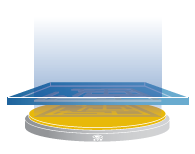
Mask aligners, for example, involve the pattern being directly exposed onto a substrate through a mask. This mask remains in close proximity to the photo-sensitive, resist-coated wafer. Minimum pattern size is dictated by the exposure gap present between the wafer and mask. A smaller gap between the mask and resist surface will enable smaller patterns; but if the gap is too close then this can cause mask contamination, ultimately resulting in yield issues.
Minimum resolution in production is limited to several microns, but despite this limitation, mask aligners can offer solutions for low-cost, high-throughput patterning, particularly in applications requiring high exposure dose and thick photoresists or wafer-level designs.
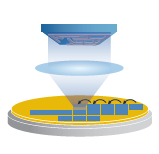
In order to address these process difficulties, back-end-of-line (BEOL) steppers employ projection optics between a mask/reticle and wafer, allowing manufacturers to pattern smaller feature sizes without the risk of contamination.
As the optical design of the complex objectives and the exposure field size are restricted, exposure will occur sequentially or step-wise, with strong accelerations occurring between exposures.
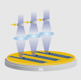
Both mask aligners and steppers are mask-based, meaning that masks incur considerable additional costs to the overall patterning process, on top of the limitations already discussed. One approach to mitigating the issue of mask cost is to employ laser direct imaging technology, utilizing individual or multiple laser beams to expose small geometrical elements in a sequential manner. The sequential nature of the exposure results in considerable cost and low throughput, even considering the advantages of direct imaging techniques.
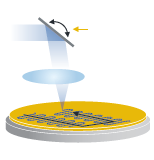
MLE™ technology works by exposing one or more wide strips in a parallel scanning fashion. By doing so, it can accommodate any size of wafer up to panels via a tightly integrated clustered write-head configuration. MLE™ technology supports all commercially available resists thanks to its high-power multi-wavelength UV source.
Throughput remains independent of resolution and layout complexity, with MLE™ maintaining the same high patterning performance regardless of photoresist. MLE™ successfully complements EVG’s range of other lithography systems, targeting new and emerging use cases where other approaches may succumb to limitations in scalability or CoO.
Working with Novel Lithography Schemes
EVG’s MLE™ technology pushes the limits of existing lithography systems. MLE™ technology facilitates high-resolution (<2 microns L/S), stitch-free, maskless exposure of the complete substrate surface coupled with low CoO and high throughput.
The system is scalable in line with user needs. This is achieved by adding or removing UV exposure heads as required, facilitating rapid transition from R&D to HVM mode. Throughput optimization is straightforward, and the system can be easily adapted to work with different substrate sizes and materials. It is ideal for processing a range of substrates, ranging from small silicon or compound semiconductor wafers up to panel sizes.
MLE™ can maintain robust patterning performance regardless of photoresist. This is due to a scalable and flexible high-power UV laser source, which offers a range of wavelength exposure options.
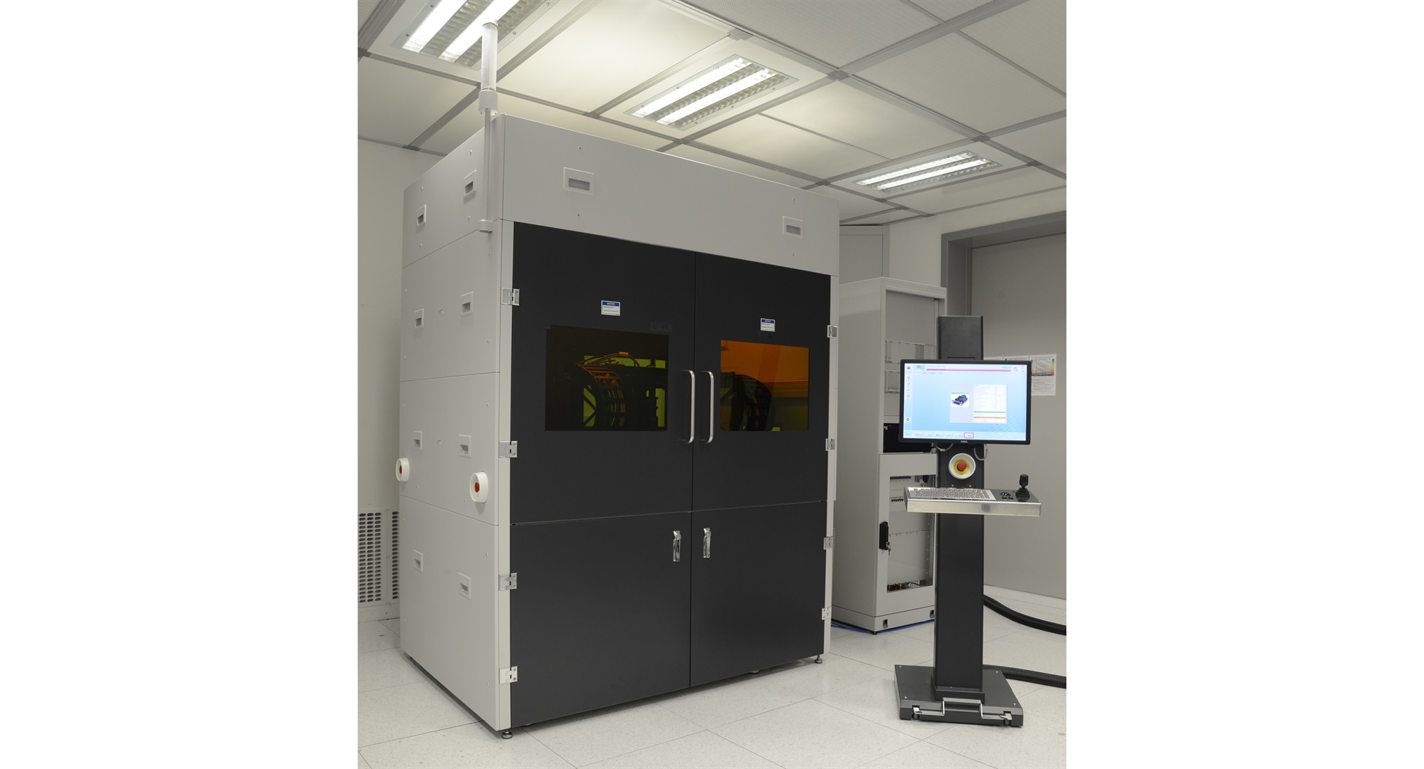
Image Credit: EV Group
Unsurpassed Flexibility, Scalability and Cost-of-Ownership Benefits
MLE™ technology helps users avoid increasing mask costs related to multiple chip designs and mask inventory management, both of which have a considerable impact on overall development and production costs. A further demand in back-end lithography centers around a reduction in the effect of pattern variability (in terms of materials diversity and substrate sizes) on time to market.
MLE™ technology is a scalable means of patterning any substrate shape, ranging from different wafer sizes to panels. The demo-ready technology utilizes clustered multi-wavelength laser light sources that operate at 375 nm and/or 405 nm wavelengths. These facilitate thin resist patterning; for example, positive and negative resists, dry film resists, polyimides, PCB patterning, thick resist exposures supporting high aspect ratios (typically found in wafer-level packaging), microfluidics, MEMS structuring and integrated silicon photonics applications.
As well as mask-related issues, current mask-based technologies also have limited control of distortions, causing them to face process difficulties linked to high-order substrate deformations.
Unlike current mask-based technologies, MLE™ technology can accommodate high substrate stress, bow and warp. This is due to the technology’s integrated dynamic alignment capabilities, and its ability to adjust to substrate material and surface variation while actively compensating for stress-induced inaccuracies (for example, rotation, expansion, shift, and high order distortion errors) and mechanical die placement.
MLE™ technology also simultaneously enables real-time digital/‘binary’ wafer-level-layout and individual-die-layout patterning. It is especially suited for ad hoc individual die annotation, encryption key and serial number implementation. Programmable modulations of UV dosage during the patterning process help facilitate resist thickness level variation following the development process.
This unique feature enables complex 3D multi-level resist patterns to be fabricated. These patterns are applicable in future MEMS, novel photonic devices or refractive/ diffractive micro-optical elements. It is possible to store the digital programmable die/wafer layout in a range of industry standard vector file formats including GDSII, OASIS, Gerber, ODB++, and BMP.
The vector layout is computationally processed (rasterized) within a few seconds before being stored in bitmap format. As a result, neither resist type (positive or negative), exposure dose level or associated design layout complexity will affect the speed of the patterning process.
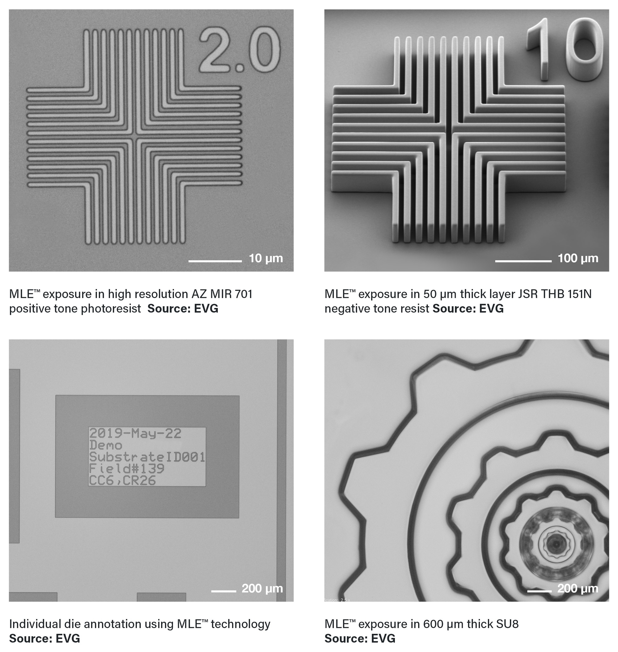
Image Credit: EV Group
Towards a New Digital Infrastructure
With the novel MLE™ (maskless exposure) technology, EV Group’s goal is to introduce a new lithography tool to the market, while simultaneously addressing a trend towards agile, smart digital processing in the semiconductor industry. The company’s other key goal in this endeavor is the delivery of unique maskless scalability in terms of throughput, format and related consumables-free infrastructure.
This state-of-the-art exposure technology also allows manufacturers operating in novel markets to address challenges associated with the deployment of flexible substrates or new materials.
The virtually unlimited design flexibility afforded by this novel technology opens up current – highly conservative - environments to new innovations while simultaneously helping to reduce development cycles, and bridge the gap between R&D and HVM. This is made possible due to exactly the same technology being available to both fields.
The global semiconductor market is highly competitive, with manufacturers requiring scalability, flexibility, efficient development and carefully managed operational costs. All of these factors are essential in reducing time-to-market and expanding market share, ultimately helping companies to deliver ground-breaking solutions to end-customers.
At its core, this new digital infrastructure facilitates dynamic device innovation while ensuring that costs are kept at a reasonable level.
This information has been sourced, reviewed and adapted from materials provided by EV Group.
EV Group (EVG) is a leading supplier of high-volume production equipment and process solutions for the manufacture of semiconductors, MEMS, compound semiconductors, power devices and nanotechnology devices.
A recognized market and technology leader in wafer-level bonding and lithography for advanced packaging and nanotechnology, EVG’s key products include wafer bonding, thin-wafer processing and lithography/nanoimprint lithography (NIL) equipment, photoresist coaters, as well as cleaning and inspection/metrology systems.
With state-of-the-art application labs and cleanrooms at its headquarters in Austria, as well as in the U.S. and Japan, EVG is focused on delivering superior process expertise to its global R&D and production customer and partner base – from the initial development through to the final integration at the customer’s site.
Founded in 1980, EVG services and supports an elaborate network of global customers and partners all over the world, with more than 1000 employees worldwide and fully-owned subsidiaries in the U.S., Japan, South Korea, China and Taiwan.
For more information on this source, please visit EV Group.