Sponsored by EDAXFeb 7 2023Reviewed by Olivia Frost
Electron Backscatter Diffraction (EBSD) has been extensively used for orientation and microstructure characterization of crystalline materials, including metals, ceramics, and minerals.
With advancements in EBSD detector technology, there is a growing interest in utilizing EBSD analysis on beam-sensitive materials, such as organic photovoltaics and biominerals. These materials can be easily damaged by high-intensity electron beams, making traditional EBSD impossible.
The Clarity™ EBSD Detector, the first direct electron detector for EBSD applications to be commercially available, offers a solution to this problem by allowing for true low-dose EBSD analysis. This opens up the possibility for the characterization of these types of crystalline materials.
Results and Discussion
To maximize the potential of EBSD data collection while minimizing high tension and electron dose, it is crucial to understand the amount of signal required to generate an indexable diffraction pattern.
Dynamic simulations of the diffracted signal indicate that patterns with a low electron density, such as one electron per pixel on average, can already produce indexable patterns (as illustrated in Figure 1).
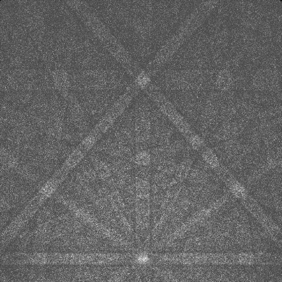
Figure 1. Simulated Si EBSD pattern with an average of one electron per pixel using only diffracted electrons. Image Credit: EDAX.
It is important to note that a significant portion of an EBSD pattern signal is comprised of background electrons, which are scattered at the sample surface and reach the detector without contributing to the bands in the pattern.
The ratio between electrons in the bands and background electrons determines the minimum required electron dose. The unprocessed EBSD patterns of Be and Au (shown in Figure 2) demonstrate this difference.
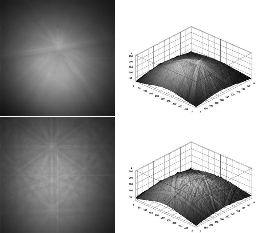
Figure 2. Unprocessed Be (top) and Au (bottom) EBSD patterns with corresponding 3D intensity plots. Image Credit: EDAX.
The bands in the diffraction pattern of Au are easily visible and approximately 20% brighter than the background signal. In contrast, the bands in the Be pattern are very weak and barely distinguishable from the background intensity cone.
This illustrates that a higher electron dose is required to obtain an indexable pattern for Be compared to Au. EBSD patterns of materials with an average atomic number typically exhibit a band-to-background ratio of around 1:10.
As one electron per pixel in the diffracted signal is enough to see the bands, an average electron dose on the EBSD detector of 10 electrons per pixel is indexable (as shown in Figure 3).
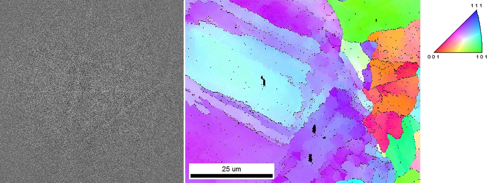
Figure 3. (left) EBSD pattern with average 10 electrons per pixel and (right) IPF map of 3D printed steel collected using 13 pA beam current. Image Credit: EDAX.
It is important to note that the above-mentioned scenario works under ideal conditions of perfect crystal and no signal loss. In practice, this means that reliable indexing can be achieved with an electron dose of 20-50 electrons per pixel on most materials.
Additionally, the overall intensity of observed EBSD patterns is also influenced by the material's backscatter coefficient. Light materials produce less intense EBSD patterns and have a lower fraction of electrons that carry diffracted information, thus requiring a longer exposure to the electron beam (as shown in Figure 4).
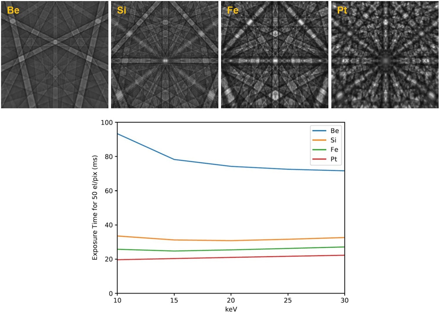
Figure 4. Simulated EBSD patterns and chart illustrating the different diffracted intensities and required exposure time to reach an average of 50 diffracted electrons per pixel using 100 pA beam current at different kV - assuming ideal crystal, surface, and detection efficiency. Image Credit: EDAX.
For experimental patterns, the required exposure time increases as the electron energy decreases (Figure 5). The curves in the chart demonstrate that the required exposure times remain constant at beam energies above 20 kV but increase with decreasing electron energies.
This is the result of a combination of the diffracted intensity and the lower EBSD detector efficiency at decreasing kV.
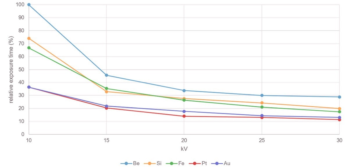
Figure 5. Experimentally determined exposure times for different materials at constant beam current. Image Credit: EDAX.
The effects mentioned above establish a clear limit for the minimum electron dose required to analyze metals. Minerals and ceramics, which are typically lighter, may require slightly more signal.
Biominerals and crystals containing organic components, such as certain photovoltaic perovskites, pose an additional challenge. In many cases, organic material is present between or incorporated within the crystals of interest.
Organic structures, such as those present in certain biominerals and crystals containing organic components, may disintegrate upon exposure to high-intensity electron beams. This damage and contamination can prevent successful EBSD phase and orientation analysis. Minimizing the electron dose can mitigate these effects.
The interest in low-dose EBSD analysis is driven by two main applications:
- Minimizing the interaction volume in the sample to improve lateral resolution
- Enabling orientation analysis of beam-sensitive materials.
The examples provided below demonstrate the use of a Clarity EBSD detector and off-line NPAR™ processing to maximize indexing performance in areas with rough surfaces.
Figure 6 depicts the microstructure of an Atrina Pectinata shell at the transition region from calcite to aragonite nacre. Mollusk shells, particularly aragonite nacre, are very sensitive to energetic electrons and require low-dose settings for optimal investigation.
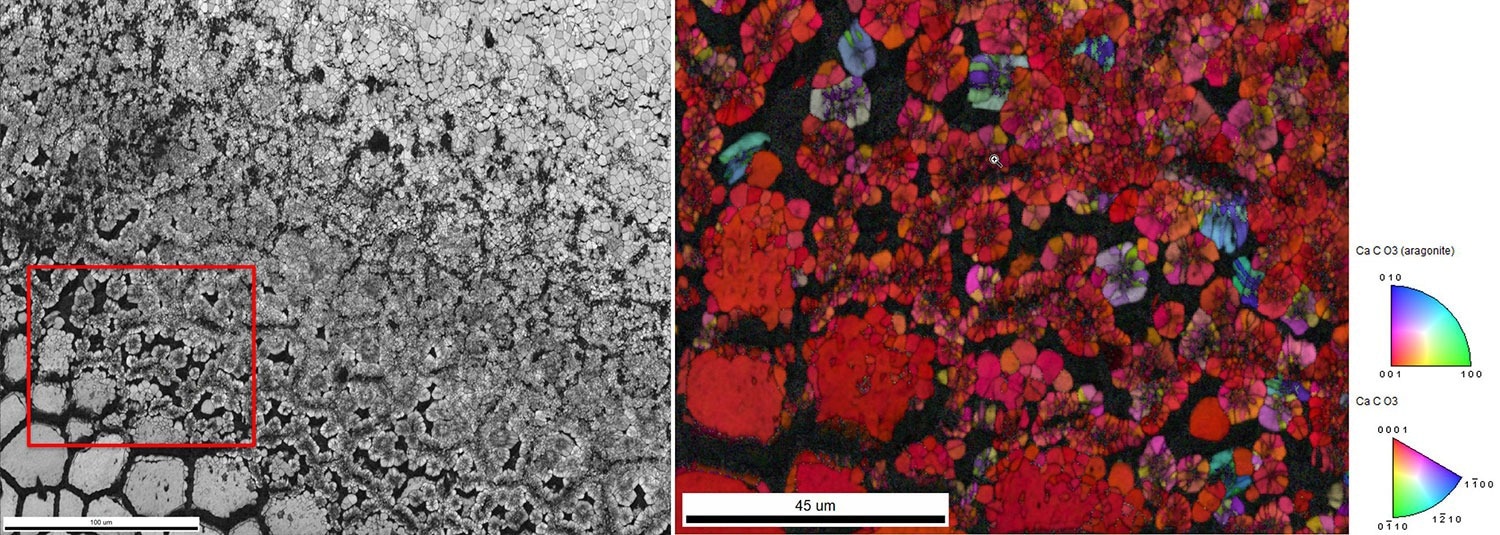
Figure 6. (left) EBSD Image Quality map showing the transition zone from columnar calcite (lower left) to planar aragonite nacre (top right). (right) The detailed Inverse Pole Figure map illustrates the grain microstructure directly at the calcite-aragonite contact. Image Credit: EDAX.
At the boundary between calcite and aragonite, a complex microstructure of calcite subgrains that appear to be correlated with aragonite grains of similar size is observed. The aragonite grains initially form along the edges of the calcite crystals and then merge to form full polycrystalline covers of the columns.
As a final step, small aragonite crystals are covered by equiaxed planar aragonite crystals that form the smooth nacre structure coating the inside of the shell. The initial formation of aragonite between the calcite pillars was visualized in detail using a 12 kV, 250 pA electron beam (as shown in Figure 7).
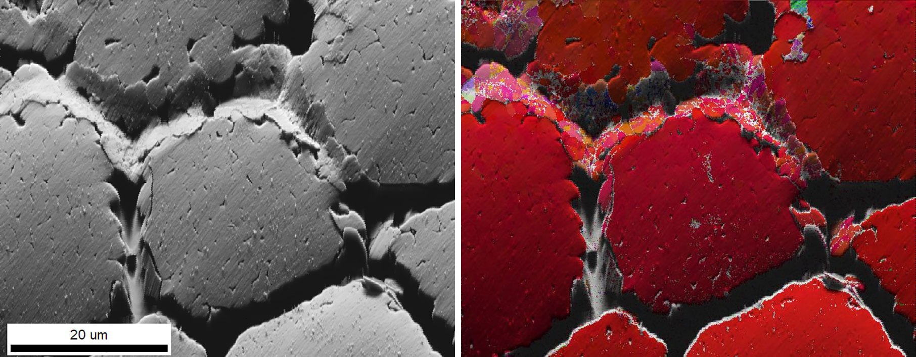
Figure 7. (left) Image Quality (IQ) map with (right) superimposed IPF map of aragonite platelets in between calcite pillars. Image Credit: EDAX.
Low-dose EBSD is also necessary to investigate different perovskite materials for their photoelectronic properties. Figure 8 illustrates the microstructure of an inorganic halide perovskite (CsPbI3).
The SEM image shows sintered grain aggregates on a glass substrate with a radial structure radiating from a central point. EBSD was utilized to assess if these clusters preserved numerous orientations, reflecting the original crystal orientations before sintering, or whether the sintering process comprised complete recrystallization.
The IPF colors in Figure 8 indicate that most clusters display only a single color, thus confirming that full recrystallization has occurred.
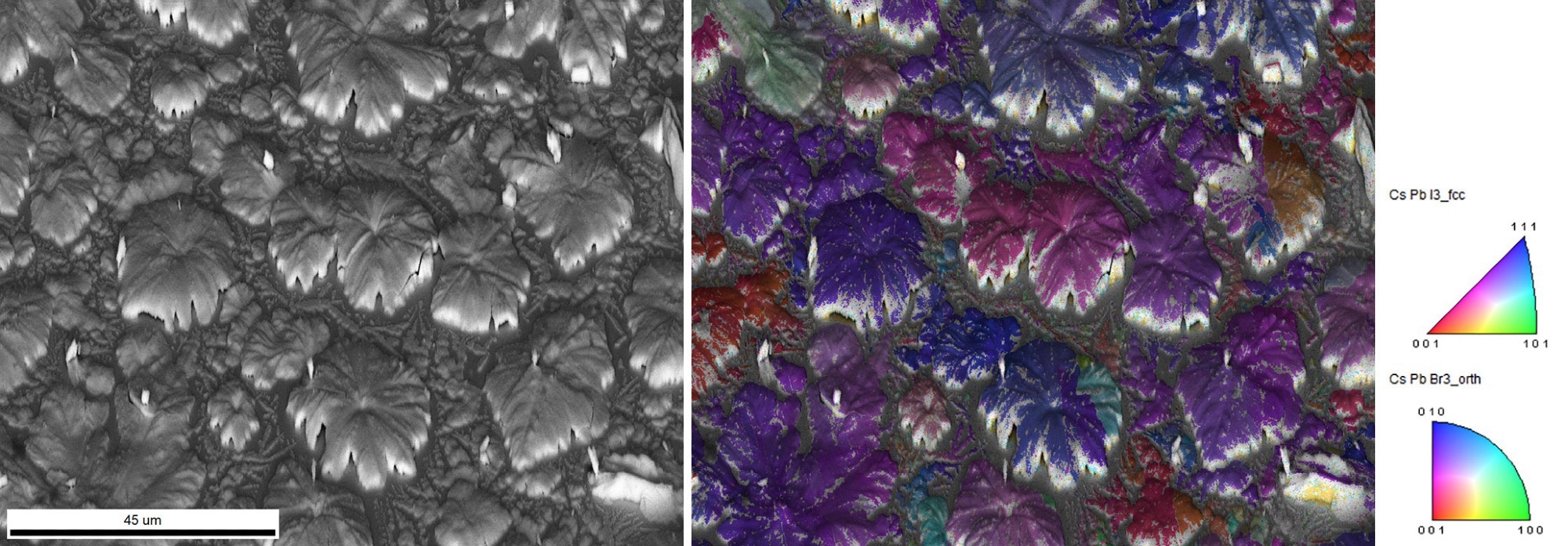
Figure 8. (left) SEM image and (right) IPF map of CsPbI3 halide perovskite collected using 15 kV and 300 pA electron beam. The larger grains are an orthorhombic phase; in between these grains, a small fraction of a cubic phase was observed. Sample courtesy of Dr. Julian Steele (KU Leuven, Belgium). Image Credit: EDAX.
Conclusion
The beam intensity limit for low-dose EBSD is determined by the ratio of diffracted bands to the background signal, which increases with the backscatter coefficient of the material.
Indexable EBSD patterns may be created with as little as 10 electrons per pixel for materials having diffraction intensities comparable to iron alloys. A minimum of 20-50 electrons per pixel is necessary for lightweight materials.
The EDAX Clarity Direct Electron Detector is particularly well-suited for investigating beam-sensitive materials under low-dose conditions that minimize damage to sensitive materials.

This information has been sourced, reviewed and adapted from materials provided by EDAX.
For more information on this source, please visit EDAX.