For decades, optical microscopy has been restricted by diffraction limits, making it difficult to resolve nanostructures. Electron microscopy (EM) is the current standard for high-resolution imaging, but it has drawbacks such as extensive sample preparation, high costs, and inability to do fast, repetitive scans.
The incorporation of the SMAL (Super-resolution Microscopy Assisted Lens) in the Nanoro platform solves these problems, overcoming the gap between optical and electron microscopy.
This following presents the SMAL lens's performance in semiconductor imaging, highlighting its ability to resolve features down to the tens of nanometers with exceptional clarity.
Demonstration on a Semiconductor Sample
To test the resolving capability of the SMAL lens, a semiconductor microchip from an Intel i5 processor was chosen as a test sample.
With its nanoscale characteristics, this type of sample is ideal for resolution demonstrations and is typically analyzed using a scanning electron microscope (SEM).
- The DRY SMAL lens on the Nanoro M and Nanoro Generation systems allowed for clear visibility of 80 nm features evaluated independently by SEM.
- The Nanoro Generation's Blue Mode enhances resolution, highlighting microscopic features with remarkable sharpness in optical microscopy.
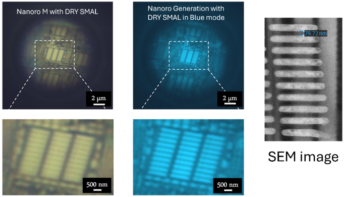
Image Credit: LIG Nanowise Ltd.
These findings highlight how optical microscopy, when supplemented with SMAL technology, can approach electron microscopy's resolution range while maintaining the convenience and flexibility of light-based imaging.
Comparative Imaging Analysis
To demonstrate the advantages of the SMAL lens, a direct comparison was carried out between two imaging configurations:
- A scan taken with the Nanoro Generation in Blue Mode and a DRY SMAL lens.
- A scan taken with a standard 100x objective lens.
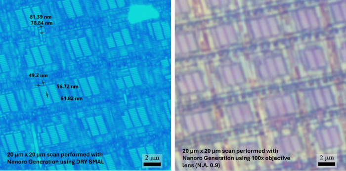
Image Credit: LIG Nanowise Ltd.
The difference in depth and contrast is significant. While the 100 x objective produces a distinguishable image of the microchip surface, the SMAL lens shows nanoscale details with even better precision.
Another significant advantage is in the workflow. The Nanoro software allows users to capture high-resolution scans in minutes, minimizing the time required for nanoscale analysis. In addition, the software's integrated measurement tool enables exact feature quantification, ensuring data acquisition reliability and reproducibility.
Conclusion
This article presents the potential of SMAL lens to transform optical microscopy. Its technology pushes the limits of the possibilities of light-based imaging systems by resolving features as small as 80 nm and beyond.
The SMAL lens, when used with the Nanoro Generation in Blue Mode, provides:
- SEM-like resolution without the complexity of electron microscopy
- Fast acquisition times, allowing efficient workflows
- Integrated high-precision measuring instruments for robust analysis
Able to conduct nanoscale imaging quickly and accurately, Nanoro is highly useful for semiconductor research, materials science, and advanced manufacturing applications that require both speed and resolution.

This information has been sourced, reviewed, and adapted from materials provided by LIG Nanowise Ltd.
For more information on this source, please visit LIG Nanowise Ltd.