Artificial intelligence (AI) is no longer just about software; it is now radically transforming the semiconductor industry. As AI workloads rise, new requirements emerge for processing power, memory bandwidth, and energy efficiency, prompting a significant revolution in semiconductor architecture.
In this context, the industry is moving beyond typical transistor scaling and toward system-level innovation. Performance enhancements are now achieved through improved packaging, novel materials, and the combination of various types of components.
This transition results in more powerful but also more complex devices with more interfaces and potential failure points, necessitating more advanced, practical testing techniques.
From Monolithic Chips to 3D-Integrated Systems
Modern electronics use complex packaging architectures, moving from traditional 2D chips to 2.5D designs with chiplets and interposers, and eventually to completely 3D-stacked devices.
These innovative designs boost performance by bringing processors, memory, and connectors closer together. However, as more functions are bundled into a single package, the number of interfaces and potential failure points increases dramatically.
This modification incorporates co-packaged optics and complex material layers, transforming the "package" into a highly integrated system. As a result, testing must go beyond evaluating individual components and instead include approaches that reflect how the entire system operates in real-world scenarios.
The Instron® 6800 Series universal testing systems are designed specifically for this change, combining component-level materials testing and system-level reliability validation on a single, customizable platform.
Engineers can adapt to new architectures by using interchangeable grips, fixtures, and environmental attachments rather than investing in completely new equipment.
The Materials Driving Innovation and the Challenges They Are Creating
Manufacturers are introducing novel materials to facilitate 3D integrations, including improved adhesives, thermal interface materials (TIMs), and glass substrates. These enable larger, more integrated designs and improved thermal performance, but they also introduce new risks that necessitate focused testing methods.
Key Challenges Include:
- Coefficient of thermal expansion (CTE) mismatch between layers
- Warpage and stress buildup
- Risk of fracture in brittle materials such as glass
- Sensitivity to thermal cycling and environmental factors
Each of these failure types demands a different test procedure. Tensile testing determines how adhesives function under pull-out loads; flexural testing measures fracture behavior on brittle substrates; and shear testing assesses bonded interface integrity.
The Instron 6800 Series supports all of these on a single frame with replaceable grips and fixtures, which is crucial as material sets advance and qualification cycles decrease.
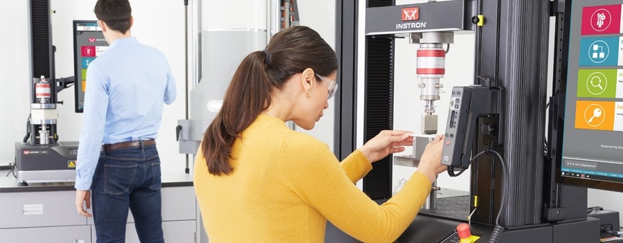
Image Credit: Instron - USA
Thermal Management as a Defining Design Constraint
As AI-powered devices increase power density, thermal management has become one of the most critical restrictions in semiconductor design.
Heat has a direct impact on performance and reliability in advanced packaging, where numerous dies and optical components are tightly integrated, especially in stacked arrangements with restricted heat dissipation.
Testing must simulate real-world conditions rather than just ambient surroundings. This means combining thermal cycling with mechanical stress and observing how materials react to localized temperature variations over time.
Engineers can analyze adhesives, TIMs, and bonded interfaces using integrated environmental chambers and Instron testing equipment, which simulate the conditions these materials would face in service. This integrated technique identifies failure situations that ambient testing may overlook.
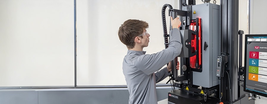
Image Credit: Instron - USA
Moving Beyond Component Testing to Real-World Simulation
Testing has evolved from assessing material attributes in isolation to understanding how materials operate in their intended application setting. Engineers today require solutions, so they need to ask not just "How strong is this material?" but "How does it behave in this assembly, under these loads, at this temperature?"
Application-Specific Test Methods Include:
- Die-shear testing to ensure connection and adhesive integrity
- Conducted micro-bend tests to evaluate die strength and fracture behavior
- PCB and package bend testing to simulate assembly and operating loads
Dedicated fixtures, such as Instron's die-shear and micro-bend fixtures, enable these tests by ensuring exact alignment and repeatable orientation.
Because they are designed for use with Instron universal testing systems, they may quickly switch between test techniques on a single system, minimizing the number of specific instruments required and shortening qualification schedules.
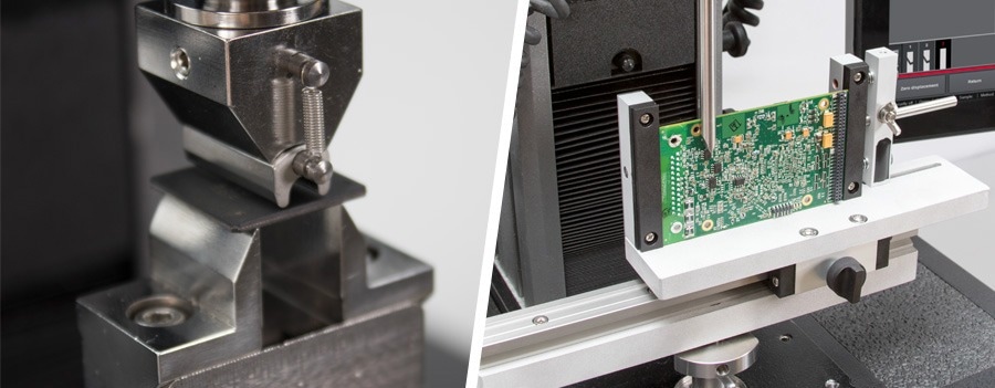
Image Credit: Instron - USA
Multi-Physics Data: Testing Mechanical, Thermal, Electrical, and Optical Behavior Together
As semiconductor systems become increasingly complex, testing must capture behavior across multiple domains at once. Measuring mechanical responses alone is no longer enough; engineers must understand how force, displacement, temperature, electrical performance, and optical signal quality interact.
This is especially important in systems that combine silicon photonics and co-packaged optics, as optical components require exceedingly fine alignment. Even minor mechanical changes induced by thermal expansion or assembly stress can impair signal transmission.
CTE mismatch between materials in AI systems that mix optics with high-power components can produce progressive misalignment over repeated thermal cycles, a failure mechanism that is only observable when mechanical and optical data is evaluated simultaneously.
Instron systems powered by Bluehill® Universal software directly address this issue. Bluehill software enables simultaneous acquisition of mechanical, thermal, electrical, and optical data streams in real time, with automated test sequences, exportable reports, and support for third-party sensor integration.
From a single test run, engineers can detect coupled failure sources, validate simulation models, and gain a comprehensive understanding of system behavior.
Scaling Semiconductor Testing for High-Volume Manufacturing
AI infrastructure growth is generating increased production volumes, putting pressure on manufacturers to test more samples faster while maintaining data quality. As complexity grows, manual testing methods become a bottleneck, increasing operator variability and restricting throughput.
Automation is a key enabler. Automated XY stages and other technologies provide reproducible, high-throughput testing with minimal operator intervention. When combined with automated test sequences in Bluehill Automation software, these methods enable continuous or unattended testing while ensuring data consistency across high-volume runs.
For manufacturers increasing AI hardware production, combining a universal testing platform with automation-ready hardware and software allows testing capacity to grow in tandem with production volume without incurring commensurate cost or manpower increases.
AT2 Automated XY Stage | Configured for Flexural Testing of Microelectronics
Video Credit: Instron - USA
A Configurable Platform for a Rapidly Evolving Industry
Semiconductor research is accelerating. New materials, architectures, and integration approaches are emerging faster than most laboratories can keep up with, and adding dedicated equipment for each new test requirement is not a viable solution.
In this setting, a single adaptable platform that can develop to meet new demands provides a significant advantage over a growing collection of single-purpose instruments.
The 6800 Series is built to accommodate this reality, with interchangeable fixtures and grips, support for third-party sensor integration, integrated environmental chambers, and automation-ready hardware and software.
One platform can handle die-shear and micro-bend fixtures for microelectronics applications, as well as whole-system-level assemblies tested under combined heat and mechanical strain.
As AI pushes the limits of what semiconductor devices can do, testing must keep up and become more integrated, application-specific, and scalable.
Instron's modular platform, which includes the universal testing machine, application-specific fixtures, and Bluehill software, is designed to expand alongside semiconductor innovation, providing engineering teams confidence that their reliability data accurately reflects the real world.

This information has been sourced, reviewed, and adapted from materials provided by Instron - USA.
For more information on this source, please visit Instron - USA.