Silicon (Si) is widely used in the production ICs and solar cells. Although many different technologies are used in the latest developments, lithography is the traditional technique to fabricate the structures in semiconductor devices. Achieving high quality devices is possible by reducing stress and stress-induced artifacts in the devices. Other structures involving the growth of layers, with different lattice constants, on top of each other require the strain for lattice matching.
Raman measurements can effectively analyze the strain state of crystalline materials, thereby providing an efficient and nondestructive way of developing the most suitable production processes. This article discusses the analysis of structures in crystalline Si written by laser lithography using an alpha300 RA Confocal Raman-AFM that integrates AFM, Confocal Raman Imaging and Confocal PL Imaging in a single instrument.
Experimental Procedure
In the alpha300 RA Confocal Raman-AFM, a piezoelectric scanning stage was used to achieve the XY positioning of the sample for scanning and lithography and a stepper motor was employed for the focus control (10nm single step). Using this innovative system, all experiments could be carried out as follows:
Lithography
The pulsed 532nm laser featured in the alpha300 RA Confocal Raman-AFM was applied for laser scribing in conjunction with the DaVinci Lithography package. The scripting function of the lithography package facilitated not only moving the sample arbitrarily in XY but the microscope upward when a movement without laser scribing is preferred.
Confocal Raman Imaging
An additional frequency doubled Nd:YAG 532nm laser was employed for confocal Raman imaging which yielded 20mW optical power. The use of a 100X NA 0.9 objective facilitated the laser to focus on a diffraction-limited spot with a 355nm diameter. The signal was acquired utilizing a 25µm core diameter optical multi-mode fiber, which served as a pinhole to obtain the optimal depth resolution.
A UHTS 300 spectrometer in conjunction with a back-illuminated CCD camera and an 1800g/mm grating was employed for detection using an acquisition time of 12.2ms/spectrum. Two scans were carried out on the laser transcribed area: A planar scan in the XY area (50x50µm2 with 200x200 points) and a depth scan in the XZ plane (20x5µm2 with 200x50 points).
Confocal PL Imaging
Confocal PL imaging was performed with the same laser used for Raman imaging, but with a specially selected 50X NA 0.8 objective that facilitated optimal throughput for the PL signal (in the range of 1000 - 1250nm for Si) and minimal chromatic aberration between the PL peak and excitation wavelength (532nm). The signal was collected by a 100µm core diameter multi-mode fiber and delivered to a SpectraPro 2300i mirror based spectrometer by a 150g/m grating and an InGaAs CCD camera 1024 pixels in width. A scan of 50x50µm2 with 100x100 points and an integration time of 0.210s/spectrum was conducted.
Atomic Force Microscopy
AFM measurements were taken in AC mode utilizing a force modulation cantilever (Nanoworld) with a resonance frequency of 87kHz. The first overview scan was done on an area of 50x50µm2 with 512x512 points and the second scan on an area of 14x14µm2 with 256x256 points.
Experimental Results
At this laser power, it took roughly 2 minutes to write the structures using a lithography process. Following this, the white light image as depicted in figure could be observed. The image was stored with the WITec Control software utilizing the integrated video camera. Subsequent to the planar confocal Raman image scan, it is possible to extract Figure 2a from the integrated intensity of the first order Si band near 520rel.1/cm.
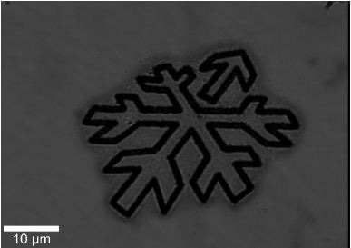
Figure 1. White light image of the lithographically written structure in Si.
Figure 2b illustrates the intensity profile along the blue cross section displayed in Figure 2a. The cross section shows a FWHM of the intensity profile of 680nm. The same structures were then scanned with a diffraction-limited resolution. The detected structures are faintly bigger than diffraction-limited. This could be due to differences in the sample height, shown as brighter and darker areas in Figure 2a. The green line in Figure 2a represents where the depth scan took place.
![Confocal Raman Image of the intensity of the first order Si line [a] and the intensity profile along the cross section marked in blue [b].](https://d12oja0ew7x0i8.cloudfront.net/images/Article_Images/ImageForArticle_10575_44895995813611116318.jpg)
![Confocal Raman Image of the intensity of the first order Si line [a] and the intensity profile along the cross section marked in blue [b].](https://d12oja0ew7x0i8.cloudfront.net/images/Article_Images/ImageForArticle_10575_448959958181258878.jpg)
Figure 2. Confocal Raman Image of the intensity of the first order Si line [a] and the intensity profile along the cross section marked in blue [b].
Figure 3a shows the integrated intensity of the first order Si peak, revealing that the origin of the intensity is from roughly the same height and only very little signal is originating from the positions of the laser transcribed structures. The brighter areas located near the structures are in line with the results shown in Figure 2a, where higher intensity is determined near the structures. Figure 3b delineates the intensity profile extracted along the turquoise line. The sharpness of this profile is owing to the high depth resolution possible with the alpha300 RA Confocal Raman-AFM and the limited penetration depth of the laser light into Si.
![Confocal Raman Image of the intensity of the first order Si line along a depth scan [a] and the intensity profile along the cross section marked in turquoise [b].](https://d12oja0ew7x0i8.cloudfront.net/images/Article_Images/ImageForArticle_10575_448959958224884254881.jpg)
![Confocal Raman Image of the intensity of the first order Si line along a depth scan [a] and the intensity profile along the cross section marked in turquoise [b].](https://d12oja0ew7x0i8.cloudfront.net/images/Article_Images/ImageForArticle_10575_448959958271643556871.jpg)
Figure 3. Confocal Raman Image of the intensity of the first order Si line along a depth scan [a] and the intensity profile along the cross section marked in turquoise [b].
The data collected in the planer and depth scan was studied in terms of peak shift of the first order Si peak to analyze the strain state of the Si around this structure, using the advanced fitting option in the WITec Project Plus software. The spectra were fitted using a Lorenzian curve.
The exact location of the peaks could be extracted from the results and is plotted for the planar scan in Figure 4a and for the depth scan in Figure 4c. Figure illustrates two representative, averaged spectra with the relevant fitted Lorenzian curves. The shift to lower wave numbers at the edges of the structures is readily apparent in both scans, indicating compressive stress in the crystalline structure at these positions.
![Confocal Raman Image of the position of the first order Si line in the planar scan [a] and in the depth scan [c]. Two representative spectra showing the shift are shown in [b].](https://d12oja0ew7x0i8.cloudfront.net/images/Article_Images/ImageForArticle_10575_44895995831504639437.jpg)
![Confocal Raman Image of the position of the first order Si line in the planar scan [a] and in the depth scan [c]. Two representative spectra showing the shift are shown in [b].](https://d12oja0ew7x0i8.cloudfront.net/images/Article_Images/ImageForArticle_10575_448959958359259254644.jpg)
![Confocal Raman Image of the position of the first order Si line in the planar scan [a] and in the depth scan [c]. Two representative spectra showing the shift are shown in [b].](https://d12oja0ew7x0i8.cloudfront.net/images/Article_Images/ImageForArticle_10575_44895995840509262801.jpg)
Figure 4. Confocal Raman Image of the position of the first order Si line in the planar scan [a] and in the depth scan [c]. Two representative spectra showing the shift are shown in [b].
Figure 5a depicts the integrated intensity of the Si PL signal and Figure 5b shows the PL spectrum itself. As observed in Figure 2a, the signal intensity is stronger near the structures. The signal was also analyzed for peak shifts, but significant change was not observed.
![Confocal PL Image of the intensity of the PL signal of Si in a planar scan [a] and a representative PL spectrum which originates from the center of the structure [b].](https://d12oja0ew7x0i8.cloudfront.net/images/Article_Images/ImageForArticle_10575_44895995844884269942.jpg)
![Confocal PL Image of the intensity of the PL signal of Si in a planar scan [a] and a representative PL spectrum which originates from the center of the structure [b].](https://d12oja0ew7x0i8.cloudfront.net/images/Article_Images/ImageForArticle_10575_44895995849317139388.jpg)
Figure 5. Confocal PL Image of the intensity of the PL signal of Si in a planar scan [a] and a representative PL spectrum which originates from the center of the structure [b].
Figure 6a illustrates an AFM overview scan and Figure 6b shows a zoomed in scan focusing on one of the arrows. Higher topography across the structure can be observed in both AFM images and the presence of dot-like structures along the written structure is readily apparent in Figure 6b. The AFM images reveal the significant structural changes took place in the Si where the laser transcribing was performed.
![AFM Scan of the structure. Overview[a] and zoomed scan onto one of the structures[b].](https://d12oja0ew7x0i8.cloudfront.net/images/Article_Images/ImageForArticle_10575_44895995857268522594.jpg)
Figure 6. AFM Scan of the structure. Overview[a] and zoomed scan onto one of the structures[b].
The dramatically lowered Si signal, close to 520 rel.1/cm in conjunction with the AFM images, suggests the destruction of the crystalline structure of the Si. In such a case, traces of amorphous Si along the structures could be observed. To confirm this, the average spectrum at a distance away from the structure and the average spectrum inside the grooves were computed from the planar Raman data set and are displayed in figure 7. The broad peak in this region suggests that the material created through the laser scribing is amorphous Si.
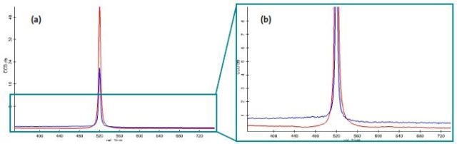
Figure 7. Raman Spectra well outside the structure (red) and inside the grooves (blue)
Conclusion
The results clearly demonstrate the ability of the alpha300 RA Confocal Raman-AFM to perform laser scribing, confocal Raman imaging, AFM imaging and confocal PL imaging on a crystalline Si sample. All analyses were controlled by the same electronics (alphaControl) and the same software (WITecControl). The written structures are readily observable with all measurement techniques.

This information has been sourced, reviewed and adapted from materials provided by WITec GmbH.
For more information on this source, please visit WITec GmbH.