In comparison to silicon, silicon carbide offers significant advantages, such as a wider band gap, higher breakdown field, and higher thermal conductivity. It is also thermally and chemically inert. These properties make silicon carbide an ideal option for use in transistors (JFETS and MOSFETs, etc.) in applications such as high temperature electronics, and in rapid high voltage devices for high temperature operation and better power transmission. It is also being used in advanced power electronics for transportation systems.
Challenges with Silicon Carbide
The properties of silicon carbide are largely influenced by the structure, quality and the number and types of impurities present in the crystal. By controlling these attributes, manufacturers of SiC raw materials and devices can enhance yield.
The Power of Raman spectroscopy
To control these parameters, the initial step is to measure them quantifiably and repeatedly. Renishaw's Raman systems are ideal for this. Analysing the laser light dispersed from the silicon carbide enables determination of crystal quality, form, and the type of defects. This can be performed quickly, easily, and non-destructively. The analysis can be performed either on a whole wafer or on a tiny region, and can provide surface and subsurface data in three dimensions (Figure 1).
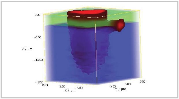
Figure 1. See subsurface features - 3D Raman image of core inclusion, showing: 3C-SiC inclusion (red); 4H-SiC epilayer (green); doped 4H-SiC substrate (blue). Sample courtesy of Prof Noboru Ohtani, Kwansei Gakuin University, Japan.
Renishaw's Raman systems can:
- Determine the presence of crystal polymorphs and polytypes (Figure 2)
- Reveal their distribution
- Determine electronic properties, such as dopant levels and free carrier concentration
- Study depth profiles, layers and interfaces
- Measure strain/stress (Figure 3)
- Map large wafers quickly (Figure 4)
- Test the complex defects in three dimensions (Figure 5)
- Be utilized for development and as QA and FA tools
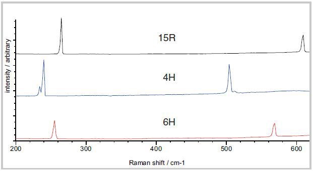
Figure 2. Determine which polymorphs and polytypes are present - Raman spectra clearly differentiate 15R, 4H, and 6H, allowing for detailed high resolution identification and mapping.
Picutre 3. Stress regions surrounding the defect (grey) and 4H/3C boundary. Compressive stresses (red), tensile stresses (blue).
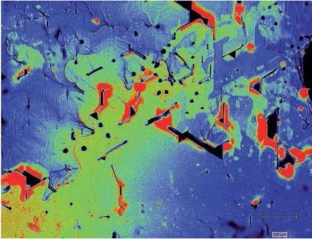
Figure 4. Large wafers in high definition - Approximately 1 mm square Raman image showing inclusions of 6H-Silicon carbide, 3C-Silicon carbide or Si (red), voids (black), and strain distribution (blue to green).
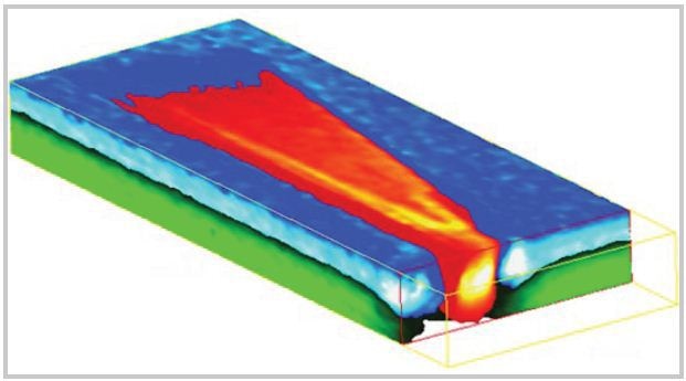
Figure 5. See defects in high detail - 'comet' defect, showing doped 4H-SiC substrate (green), 4H-SiC epilayer (blue), and 3C-SiC inclusion (red/ orange). The mapped region is 70 x 25 x 7µm3.
inVia. The Ideal Raman Tissue Imaging Tool
- The Renishaw inVia Raman microscope (Figure 6) is a research grade Raman microscope
- It features StreamLine™ imaging technology for high speed mapping, including whole wafers
- StreamLine imaging with Slalom for a rapid overview of the samples
- Surface option to obtain the best images from irregular surfaces
- High confocality StreamLineHR™ imaging reveals small details
- Queue up measurements to optimize data collection
- Can be easily switched between standard and high confocal imaging
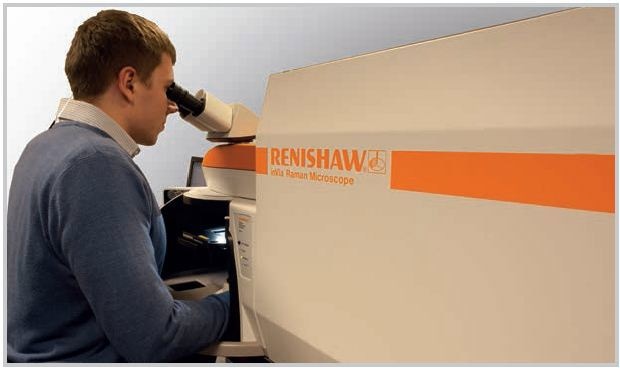
Figure 6. The Renishaw inVia Raman microscope
Q - Are researchers limited to Raman technology when measuring the properties of silicon carbide (SiC) and how do Renishaw’s Raman systems compare to alternative techniques?
No. Other techniques, such as photoluminescence are widely used. However, Raman spectroscopy gives more definitive data on polytypes and stress.
Q - How are Renishaw developing their Raman systems to offer better SiC materials for an increasing number of applications?
We’re developing new technology, such as LiveTrack focus tracking technology, that enables the analysis of samples with uneven, curved or rough surfaces, such as bowed silicon carbide wafers.

This information has been sourced, reviewed and adapted from materials provided by Renishaw.
For more information on this source, please visit Renishaw.