An important ingredient for enabling next-generation, 22 nm scale lithography is active vibration isolation technology. Based on digital signal processing algorithms and responsive piezo technology together with recent ultra-reliability enhancements, patentedi STACIS active isolators have been shown to be dependable in mission-critical fab deployment for more than 10 years.
Now, this technology is available in small form-factors suitable for new applications such as advanced microscopies and nanomanufacturing.
Vibration and Throughput: The Yield-Killers
The semiconductor industry is governed by two major laws. Moore's Law, Equation 1, describes the exponentiating density of integrated circuit elements with time.
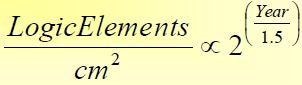
Equation 1. Moore's Law observes a doubling of device density every 18 months.
Equation 2, defines a term to describe nanoscale processing in the face of the basic economic constraint of "time is money."
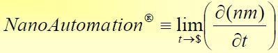
Equation 2. The economic imperative of "time is money" necessitates more devices per cm2, larger area processing and faster cycle times.
The two equations describe a challenge for researchers and process engineers: the tractability of nanoscale processes degrades with relentlessly diminishing scale, but even then the process needs to be economical. This increases substrate sizes and decreases cycle times. The two strategies are at cross purposes to the exponentiating resolutions required.
Earlier vibration isolation methodologies are not sufficient for current or future nanoscale processes. Ambient ground motion eliminates ever-finer pattern details (Figure 1) and traditional soft isolators are unable to isolate vibrations below 2 Hz and do not satisfactorily respond to onboard vibration caused by rapid processing (Figure 2). In contrast, STACIS active isolators provide strong attenuation beginning at sub-Hz levels, and is over 100 times stiffer, directly benefiting settling.
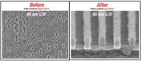
Figure 1. 45 nm line-width test patterns produced with an advanced Immersion Lithography System at SEMATECH in Austin, TX.ii (Left): Pattern is obliterated by floor vibration. (Right): STACIS isolation enables crisp, accurate photolithography. (Images obtained via SEM.)
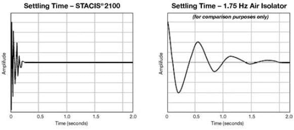
Figure 2. (Right): Settling time in response to on-board disturbance such as substrate loading is greatly improved by STACIS' novel "serial" design, helping cycle rates meet exponentiating throughput demands
The increasing needs of nanoscale processes are illustrated in recent low-threshold Generic Vibration Curves (Figure 3) - a stiff test to site engineers.
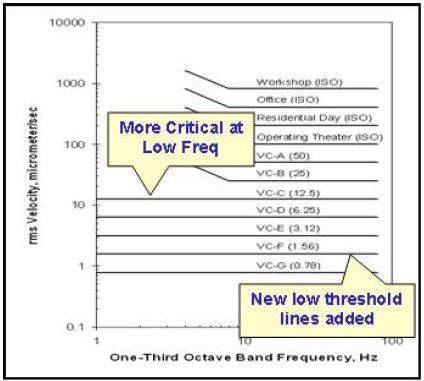
Figure 3. New, more stringent Generic Vibration Curves. Courtesy IEST RP-012, Inst. of Environmental Sciences, Rolling Meadows, IL
The STACIS Advantage
STACIS active isolators can sense the beginning of vibration in six degrees-of-freedom. They can actively nullify it by canceling actuation of stiff, piezoelectric actuators working horizontally and vertically. The necessary calculations are performed quickly with a real-time digital signal processor. This enables high bandwidth cancelation (0.6 - 250 Hz), and effectively removing latencies to minimize settling times and reducing or eliminating the effect of low frequency vibration.
The isolators have inherent stiffness, high load capacity, and clean, airless operation, and are common for OEM adaptation into leading-edge tools and for underneath-deployment in isolation platforms for sensitive devices such as optical and e-beam metrology and photolithography tools.
In addition to satisfying an essential requirement in the most recent fabs, STACIS isolators enable noisier and older fabs to accommodate the most advanced tools and at the same time ensure flexibility of floor layout and tool placement, as illustrated in Figure 4.
The STACIS isolator is also beneficial for tools already incorporating some type of internal isolation, as its novel hard-mount properties allows compatibility with the tools’ current on-board isolation methodologies.
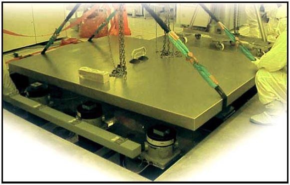
Figure 4. STACIS actuators supporting a photolithography scanner's isolation platform
In addition, smaller form-factor STACIS isolators are now available for used with small-sized instrumentation such as SEMs and advanced microscopes outside the semiconductor fab (Figure 5).
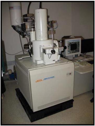
Figure 5. STACIS active isolation is newly available in smaller form-factors for instrumentation such as SEMs
The Reliable Heart of STACIS: PI's Piezo Actuators
Piezo actuators are layered devices of specialized PZT ceramic interwoven with electrodes. When voltage is applied, it causes a large-scale change in the length of the ceramic, allowing the actuators’ to be used for quick, high-force real-time position control in the nanoscale sector.
The solid-state nature of PZT ceramic distinguishes them from classical actuators. They don't need any maintenance or lubricants, and when designed and operated appropriately, they can provide unlimited lifetime service as there are no parts to wear.
This, along with the fact that they run only on electricity (with zero power needed for position hold) significantly reduces facilities and running costs and solves the thermal drift processes. Their unlimited resolution, high force, and high responsiveness make them vital to many categories of instrumentation and production equipment.
As shown in Figure 9, recent innovations have overcome traditional travel limitations, providing millimeter-level movements with sub-nanometer resolution.
Figure 6. PICMA® actuators feature patented all-ceramic encapsulation to significantly increase lifetime in challenging conditions
In principle and electrical characteristics, piezo actuators are similar to ceramic capacitors, and like them, they are reliable and durable. In creating STACIS, TMC partnered with PI to incorporate PI piezo actuators. These actuators feature novel technologies to prolong actuator life well beyond conventional benchmarks.
Recently, PI has invested in its own ceramics factory, PI Ceramic, specifically to develop piezo quality and reliable technologies, because third-party ceramics were the biggest cause of product failure. Being one of the world's biggest manufacturing set ups for ultraprecision instrumentation-grade piezo ceramics, PI Ceramic has developed several important and award-winningiii reliability innovations.
For instance, piezo ceramics were susceptible to the entry of water molecules along the layers from ambient humidity. This may limit the service life of traditional piezo actuators. Until recently, unsatisfactory efforts to cover the layered ceramics by polymer paints were the best available technologies.
With PI's patented PICMA® actuators (Figure 6)iv the all-ceramic covering provided a major leap forward, improving MTBF in humid conditions by about three orders of magnitude (Figure 7)v.
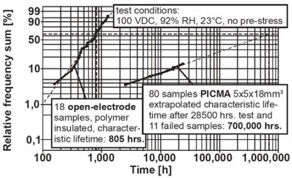
Figure 7. PICMA®'s patented construction improves MTBF by approximately three orders of magnitude in humid conditions, versus conventional polymer-encapsulated construction
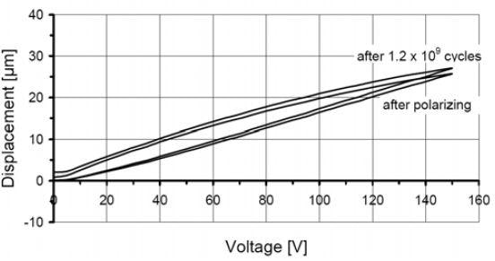
Figure 8. Open-loop piezo actuator motion characteristics remain highly consistent after more than a billion cycles
Piezo lifetime is also measurable in cycles. Figure 8 displays a characteristic performance-consistency result during open-loop actuation of a PICMA® actuator before and after more than a billion cycles. A PICMA® actuator that was being tested for a space application is available online, and has amassed 3.22 x 10¹² cyclesvi.
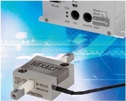
Figure 9. NEXACT® is an example of piezoceramic innovation, providing 20 mm travel with 0.03 nm resolution and 10 N force
Owning ceramics development and fabrication set ups results in other benefits in addition to improved consistency and reliability versus third-party piezo offerings. Significantly, PI's innovative skills in piezo ceramics have enabled the company to partner with companies with demanding needs like TMC.
The capability to develop new concepts in piezo ceramic actuation is also important, with unique developments such as PI's patented all-ceramic NEXACT® actuators (Figure 9) which offer 20 mm of travel with a large, 10 N push-pull force, power-off position hold capability, and resolution to 0.03 nm – suitable for sensitive positioning uses including nanoimprint lithography.
Conclusion
Two innovative industry leaders collaborated to solve challenging present-day problems and to pave the way for some of the world's most important industrial processes for the future generations. With STACIS, tool and facilities engineers concerned with isolating vibration in the face of Moore's Law's constant demands can take a rest. STACIS' new, smaller form factors will prove to be enablers for a wide array of new fields such as optical tweezers and nanomaterial studies.
References
- U.S.Patent Nos. 5660255 and 5823307 (STACIS)
- Impact of Vibration on Advanced Immersion Lithography, TMC application note
- PI Actuator Wins Circle Of Excellence Award, Photonics Spectra, January, 2005
- U.S.Patent 7,449,077
- P. Pertsch, S. Richter et al, Reliability of Piezoelectric M tors, Actuator 2006, Bremen, AXON, 2006 pp. 527-529
- PICMA® endurance testing online
This information has been sourced, reviewed and adapted from materials provided by TMC.
For more information on this source, please visit TMC.