Within this experiment, the Nexsa™ Surface Analysis System from Thermo Scientific™ was utilized to chemically locate boron nitride (BN) flakes which had been directly grown onto Cu foil via chemical vapor deposition.

The flakes’ location was quickly ascertained via XPS SnapMap. This meant that XPS spectroscopy could be used for chemical fingerprinting. Next, using co-incident Raman spectroscopy, the crystal lattice structure could be confirmed as hexagonal.
Two-dimensional (2D) materials like hexagonal boron nitride, graphene transition metal dichalcogenides, and MXenes are very much the vanguard of materials research. These materials present viable routes to new technology, in particular, electronics.1
Scientists and researchers are able to use these compounds to create a library of new materials. They do this by creating heterostructures of atomic-layer thick materials, allowing for the development of properties which are tailored for specific applications.1,2
Developing and producing this new class of materials necessitates additional advancement in technologies to accurately characterize these atomic-layer thick materials.
Nexsa Surface Analysis System.
The Nexsa Surface Analysis System is able to do this thanks to its unique integration of XPS with Raman spectroscopy, allowing it to probe the identity, impurity, crystallinity, or stress/strain or thickness of any 2D material.
Both techniques are co-incident, meaning that analysis can be undertaken from the same position, providing a thorough analysis of the sample using just one flexible instrument.
This article highlights the way in which XPS SnapMap technology (via the Nexsa Surface Analysis System) can be used to locate boron nitride flakes, which exist on a substrate’s surface at discrete locations.
It is possible to acquire a detailed chemical composition map within minutes, mapping the whole substrate and enabling rapid identification of the 2D flakes. It is then possible to acquire Raman spectra at the regions of interest, in order to study stress or strain in the 2D material or its crystal structure.
Both XPS and Raman spectroscopy are rapid non-destructive tools. A combination of both tools in a single instrument enables the user to acquire chemical information and details on molecular structure simultaneously. There is no need to transfer the samples between different instruments, and therefore no need to find the locations of interest more than once.
Experiment and Results
The position of BN flakes presents on the Cu foil was identified with XPS SnapMap (Figure 1a). Because the peak sensitivity for N1s is significantly higher than B1s, the complete sample surface was mapped for the N1s.
The total intensity of the N1s peak across the sample is illustrated in Figure 1b. This confirmed the presence of nitrogen all over the Cu substrate.
The Thermo Scientific™ Avantage™ Software (included with all XPS instruments) was used to complete a comprehensive chemical state analysis of the N1s map. This showed that nitrogen was present in two chemical states – nitride and organic nitrogen. Figure 1c and 1d show the chemical state map, plus the average XPS spectra from both chemical states of the N1s.
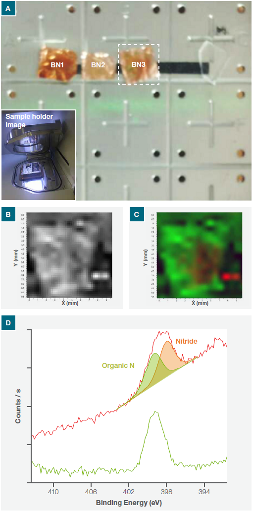
Figure 1. (a) Nexsa Surface Analysis System optical image of the whole sample platter (inset shows the sample holder in loading position), (b) N1s intensity map across the whole of the sample (c) chemical state N1s intensity map and (d) N1s average spectra from the green and red regions on the map.
A 30 μm X-ray spot size was used to produce an N1s SnapMap image. This featured the magnified area and is shown in Figure 2a, which is the optical image from the system camera.
This image corresponds to the area where nitride was visible via the low-resolution N1s image. Each pixel in the SnapMap image possesses a corresponding spectrum, allowing the user to process data identically to that of conventional XPS spectra, therefore providing the same chemical state information while showing its surface distribution.
Figure 2b displays the SnapMap of N1s, highlighting the presence of organic nitride (red region) and nitrogen (green region). A survey spectrum undertaken at the designated points (P1 and P2) in Figure 2b shows the presence of boron contribution (B1s). However, this is only from the red region and not from the green region (Figure 2c). XPS imaging has thus confirmed both the presence and the location of BN flakes.
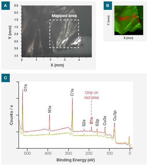
Figure 2. (a) Optical image of the sample from one of the three Nexsa Surface Analysis System cameras, (b) N1s nitride XPS SnapMap image of the mapped area and (c) XPS survey spectra at the points P1 and P2 shown in (b).
Next, high-resolution spectra of B1s and N1s were obtained, allowing for the determination of the BN flakes’ chemical states.
The B1s spectrum (Figure 3a) reveals the presence of inorganic chloride contamination, as well as peaks owing to boron nitride and boron oxynitride. Additionally, the N1s spectrum (Figure 3b) highlights the contribution from the oxynitride and nitride, verifying that the flakes were oxidized.
BN exists in two distinct polytypes: the sp2 bonded hexagonal and rhombohedral phase and the sp3 bonded cubic and wurtzite phase. Cubic BN belongs to a zinc blend type structure, with the Raman active TO phonon at 1055 cm-1 and the LO phonon at 1304 cm-1.3 Within hexagonal BN, the Raman active high energy phonon E2g is at 1366 cm-1.3
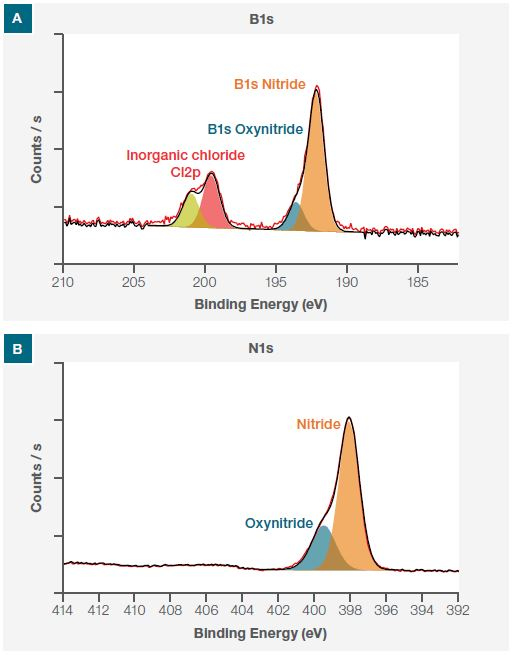
Figure 3. High-resolution deconvoluted XPS spectra of B1s (a) and N1s (b) taken at point P1 showing different chemical states.
Because of this, Raman spectroscopy is well suited for assessing a material’s structure in contrast to XPS, which provides the chemical fingerprint. Figure 4 displays the Raman spectrum at the same point - P1 (Figure 2b) - highlighting the existence of the E2g phonon mode at 1366 cm-1. This confirms that the BN flakes present on the sample are a hexagonal phase.
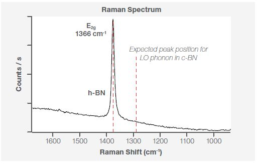
Figure 4. Raman spectra at point P1 using a 532 nm laser line.
Conclusion
This article presents a thorough chemical and structural study on BN flakes which were located at random on a copper foil substrate. The measurements presented illustrate the way in which a user can chemically locate discrete nanofeatures via the XPS SnapMap method.
This allows them to ascertain the chemistry from high-resolution XPS data, while simultaneously determining the structure and Raman spectral features using the Nexsa Surface Analysis System.
References and Further Reading
- Novoselov, K. S., Jiang, D., Schedin, F., Booth, T. J., Khotkevich, V. V., Morozov, S. V., & Geim, A. K. (2005).Two-dimensional atomic crystals. Proceedings of the National Academy of Sciences, 102(30), 10451-10453.
- Novoselov, K. S., and Neto, A. C. (2012). Two-dimensional crystals-based heterostructures: materials with tailored properties. Physica Scripta, 2012(T146), 014006.
- Reich, S., Ferrari, A. C., Arenal, R., Loiseau, A., Bello, I., & Robertson, J. (2005). Resonant Raman scattering incubic and hexagonal boron nitride. Physical Review B, 71(20), 205201.

This information has been sourced, reviewed and adapted from materials provided by Thermo Fisher Scientific – X-Ray Photoelectron Spectroscopy (XPS).
For more information on this source, please visit Thermo Fisher Scientific – X-Ray Photoelectron Spectroscopy (XPS).