Microscopy is employed in materials investigations to explore surface topology, material interfaces, substructures such as grains or intermixed phases, or the impact of various processing techniques. As such, the microscope needs to be able to handle a wide variety of material types and surface properties.
Challenges for Charged Particle Microscopes
Many technologically important materials are highly insulating. This is a challenge for charged particle microscopes. Large voltages can easily build up on samples, distorting the images, destroying contrast, and lessening image resolution.
Imaging Insulating Samples Using ORION PLUS Helium Ion Microscope
There are three methods that can be applied in the helium ion microscope to image insulating samples. The first is a charge neutralizing flood gun. This provides a diffuse beam of low energy electrons around the image field. These electrons are drawn into the positively charged area created by the ion beam, and thus a self-regulating charge compensation is maintained. The inspection of photomasks, as are used in semiconductor lithography, is an example of the application of charge neutralization. The combination of the chrome absorber and the highly insulating quartz substrate makes for a challenging system. The ORION® PLUS is able to maintain charge balance and produce a crisp image, as is seen in the example below. Important information on the chrome grain structure, the line edge roughness, and details of the chrome-quartz interface are all captured with high fidelity. We can also learn that the right-hand line is more isolated, as is understood by the fact that it is slightly darker than its neighbor.
Another method to avoid charging problems is to image via the collection of Rutherford Backscattered Ions (RBI mode). In this configuration we are capturing high energy scattered helium particles, and these are much more immune to the influence of surface potential. An example of this is seen in the investigation of thin film solar cells, shown in the second image below. The individual cells were patterned via laser cutting down to the glass substrate. Thus voltage contrast makes it very difficult to see both the conductive aluminum coating and the details of the glass surface, as is seen in the right-hand side of the image montage. The RBI mode image on the left, however, reveals the multiplicity of asperities or particles on the glass as well as the topological details of the glass itself.
Finally, there is the option for some sample types simply to image with low beam current in the ORION® PLUS, which permits charge to dissipate. The high heliuminduced secondary electron yield permits imaging with sub-picoampere beam current, which is often sufficient to create a steady charge state and thus stable imaging.
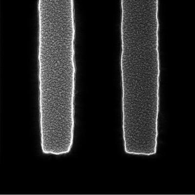
Chrome on quartz photomask (Courtesy of Dr. Mike Postek, NIST)
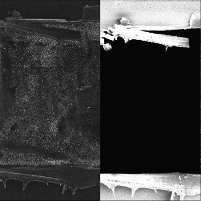
Thin film solar cell isolation cut (Courtesy of Dr. Frank Altmann, Fraunhofer Institute, Halle Germany).
ORION PLUS Capabilitites
Charge neutralization, Rutherford Backscatter Imaging
Application
Imaging insulating samples

This information has been sourced, reviewed and adapted from materials provided by Carl Zeiss Microscopy GmbH.
For more information on this source, please visit Carl Zeiss Microscopy GmbH.