Nov 17 2009
For the first time, it has been possible to measure electron density in individual molecular states using what is known as the photoelectric effect. Now published in Science, this method represents a key building block in the development of organic semiconductor elements.
Supported by the Austrian Science Fund FWF, the success of this project rested on the mathematical transformation of the measured data. This made it possible to interpret the distribution of the electrons and draw conclusions about the potential properties of organic semiconductor elements.
 A recent Science paper sheds a new light on electron density in individual molecular states.
Ultra-thin films made of organic molecules form the basis of future semiconductor technologies. Because organic molecules are extremely flexible, they can be used in a whole new range of applications, making it equally possible to create pliable screens and cost-effective solar cells. However, apart from these everyday applications for organic semiconductors, the most important task is to gain a better understanding of the interactions between organic materials and inorganic carrier substances. A team from the Universities of Graz and Leoben has now succeeded in developing a means of doing just that.
TIGHTLY PACKED
"The properties of an organic molecule are defined to a large extent by specific electron states", explains Dr. Peter Puschnig of the Chair of Atomistic Modelling and Design of Materials at the University of Leoben, who led the research. He adds: "If we can determine their distribution within the molecule accurately, then we will be able to better understand how organic semiconductor components work and thus increase their efficiency." Until now, there has been a lack of effective methods of measuring this electron distribution. Dr. Puschnig and his team have therefore succeeded in making significant progress.
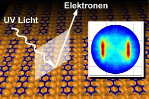
The team's achievement is based on the use of the photoelectric effect. This enables individual electrons to be "knocked out" of organic molecules. As part of this project, an organic molecule was exposed to ultraviolet light that emitted sufficient energy to separate individual electrons from the molecules. The direction and speed of the electrons thus released were then measured using highly-sensitive detectors, generating the basic data required to calculate the electron distribution within the molecule. As part of this process, Prof. Michael Ramsay and his team from the University of Graz used a hexaphenyl film just one molecule thick that had been applied to a copper surface. The team from Graz carried out the actual measurements at the Berliner Elektronen-Speicherring Gesellschaft für Synchrotronstrahlung (BESSY, Berlin Electron Storage Ring Society for Synchrotron Radiation).
A CALCULATED RESULT
Commenting on the evaluation of this data, Dr. Puschnig says: "It revealed a quite characteristic distribution of the electrons emitted. However, it initially proved difficult to interpret this distribution and it seemed it would be impossible to link the measured data to the original electron distribution in the molecule." It was only by using special mathematical transformations (Fourier Transformation) that the team was able to establish that the measured electron distribution matched that of the molecule. As the distribution was in this instance already known from calculations carried out as part of the density functional theory, it was possible to test and confirm the viability of the new method.
This new method is particularly valuable as it means measuring the behaviour of electrons at the interfaces between organic semiconductors and metals is now relatively easy and highly accurate. The study "Interface controlled and functionalised organic thin films" supported by the FWF as part of the National Research Network (NFN) is thus making a fundamental contribution to future applications of organic semiconductors.