Sep 12 2014
Excitonic dark states in single atomic layers of tungsten disulfide have been revealed by a Berkeley Lab research team using two-photon excitation spectroscopy, uncovering the reason for the exotic optoelectronic properties of monolayers of transition metal dichalcogenide (TMDC) materials.
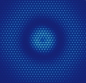 Berkeley Lab researchers have found evidence for excitonic dark states in monolayers of tungsten disulfide that could explain the unusual optoelectronic properties of single atomic layers of transition metal dichalcogenide (TMDC) materials. (Image courtesy of Xiang Zhang group, Berkeley Lab)
TMDC materials are potential two-dimensional semiconductors for photonic and nanoelectronic applications. Excitonic dark states are energy states wherein absorption or emission of single photons does not occur. Excited holes and electrons in bound pair formation are called excitons, which may cause substantial deviation between the emission and absorption energies of photons and the electronic bandgaps that allow for functioning of semiconductors in devices.
The research team deduced the excitons using ab initio calculations, and what the team found was an exotic energy sequence as well as bandgaps and excitonic binding energy that are significantly higher when compared to the previously predicted values for 2D TMDC materials.
Xiang Zhang, who led the study, said that detection of much higher excitonic binding energy and its non-hygrogenic nature as well as bandgaps in two-dimensional semiconductor materials helps in gaining more insights into the light-matter interaction as a result of intense many-body effects and the electronic and optoelectronic applications of these novel materials. Such a higher binding energy of 0.7eV holds potential to develop stable room-temperature excitons for future quantum computing applications, Zhang added.
Ziliang Ye, one of the researchers, informed that by discovering the existence of excitonic dark states in monolayers of TMDC materials, the research team demonstrated strong many-electron effects in these materials. This finding would allow for better heterostructure designs involving single atomic layers of this class of 2D semiconductors.
Besides optoelectronic applications, this finding shows promise for “valleytronics,” which pave the way for ultrafast data processing and innovative electronics.
The study results have been published in Nature.