Feb 4 2015
A research team from the University of Manchester and University of Sheffield has illustrated that 2D ‘designer materials’ can be developed to create transparent, flexible and high-efficiency electronic devices. The team headed by Nobel Laureate Sir Kostya Novoselov accomplished this feat by constructing LEDs at an atomic level. Their findings have been published in the scientific journal Nature Materials.
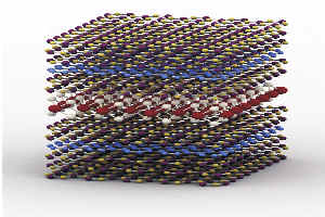 LED Heterostructure Schematic
The findings of the new research will enable graphene and associated two-dimensional materials to be used to manufacture light emitting devices for future mobile phones, TVs and tablets, making them ultra-thin, durable, adjustable and semi-transparent.
Different types of 2D crystals were combined together to form the LED device, which is capable of emitting light from its entire surface. The thinness achieved via this research work is about 10-40 atoms thick. This new device can thus be the foundation for the first generation of smart semi-transparent gadgets.
In 2004, the University of Manchester researchers were the first to explore a one-atom thick graphene sheet. Since then the material’s probable applications has been growing. It is very likely, that graphene will be first used in electronics. The discovery of other 2D materials like molybdenum disulphide and boron nitride subsequent to the discovery of graphene has opened up a whole new range of applications and research prospects.
Construction of heterostructures, (a variety of 2D materials stacked in layers) for creating bespoke functionality, and setting up quantum wells for managing the electron movement, has resulted in a whole range of probable graphene-based optoelectronics becoming achievable.
Freddie Withers, Royal Academy of Engineering Research Fellow at The University of Manchester, who led the production of the devices, stated “As our new type of LED’s only consist of a few atomic layers of 2D materials they are flexible and transparent. We envisage a new generation of optoelectronic devices to stem from this work, from simple transparent lighting and lasers and to more complex applications.”
By preparing the heterostructures on elastic and transparent substrates, we show that they can provide the basis for flexible and semi-transparent electronics.
The range of functionalities for the demonstrated heterostructures is expected to grow further on increasing the number of available 2D crystals and improving their electronic quality.
Sir Kostya Novoselov
Prof Alexander Tartakovskii, from The University of Sheffield added "The novel LED structures are robust and show no significant change in performance over many weeks of measurements.
“Despite the early days in the raw materials manufacture, the quantum efficiency (photons emitted per electron injected) is already comparable to organic LEDs.”
References