Feb 16 2016
Researchers from the University of Utah have discovered a unique 2D semiconducting material for electronics, which could produce much faster, lower power smartphones and computers.
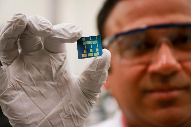 University of Utah materials science and engineering associate professor Ashutosh Tiwari holds up a substrate layered with a newly discovered 2D material made of tin and oxygen. Tiwari and his team have discovered this new material, tin monoxide, which allows electrical charges to move through it much faster than common 3D material such as silicon. This breakthrough in semiconductor material could lead to much faster computers and mobile devices such as smartphones that also run on less power and with less heat. (Photo credit: Dan Hixson/University of Utah College of Engineering)
The semiconductor is a combination of tin and oxygen, or tin monoxide (SnO). The 2D material is just an atom thick, and allows electrical charges to pass through at a faster rate compared with traditional 3D materials such as silicon. This 2D semiconducting material can be incorporated into transistors, which is the core of all electronic devices, such as graphics processors and computer processors used in mobile devices and desktop computers.
Associate professor Ashutosh Tiwari of Utah’s materials science and engineering department led the team that discovered this innovative material. The research paper was published online in the Advanced Electronic Materials journal on February, 15th. The printed version will carry this research as its cover story.
Currently, transistors and other devices found in electronic gadgets are made up of 3D materials such as silicon, and include numerous layers on a glass substrate. A disadvantage of 3D materials is that electrons bounce around in all directions within the layers. Research on 2D materials has been active for about five years. The key advantage is that the material is just one layer with the thickness of one or two atoms. As a result, the electrons “can only move in one layer so it’s much faster,” says Tiwari.
Researchers have recently discovered several types of 2D materials, such as molybdenum disulfide, graphene, and borophene. However, these materials allow movement of only N-type, or negative electrons.
To build an electronic device, a semiconductor material that allows the movement of both negative electrons and positive charges, known as “holes”, is required. Tiwari’s tin monoxide material is the first-ever stable P-type 2D semiconductor material.
Now we have everything — we have P-type 2D semiconductors and N-type 2D semiconductors. Now things will move forward much more quickly.
Ashutosh Tiwari, Associate Professor, Materials Science and Engineering, University of Utah
The latest 2D material created by Tiwari and team could lead to the manufacture of extremely small and fast transistors. Billions of transistors make up a computer processor, the more transistors inside a single chip would result in a more powerful processor. If this material is used in transistors found in smartphones and computers, it will result in speeds 100 times faster than current gadgets.
Unlike a 3D material, the electrons only have to move around in a single layer, which will reduced friction and result in the processors not getting as hot as regular computer chips. They also need very little power to operate, which is a huge advantage for mobile electronics running on battery power.
Tiwari states that the breakthrough material could also be useful for medical devices such as electronic implants, which will be able to operate for prolonged hours on a single battery charge.
The field is very hot right now, and people are very interested in it. So in two or three years we should see at least some prototype device.
Ashutosh Tiwari, Associate Professor, Materials Science and Engineering, University of Utah
Other authors of the paper include University of Utah materials science and engineering doctoral students K. J. Saji and Kun Tian, and Michael Snure of the Wright-Patterson Air Force Research Lab near Dayton, Ohio.