Apr 25 2016
Copper-indium-gallium-selenide (CIGSe) solar cells have the highest efficiency of polycrystalline thin-film solar cells. The four elements of CIGSe are vapor-deposited onto a substrate collectively to form an extremely thin layer of miniature chalcopyrite crystals. It is an exceptionally multifaceted process controlled by several variables. This is the reason why CIGSe modules in basic industrial arrangements have not yet reached the record efficiency already showcased at laboratory scale. One potential reason could be the defects formed during the fabrication process, which decrease the efficiency level.
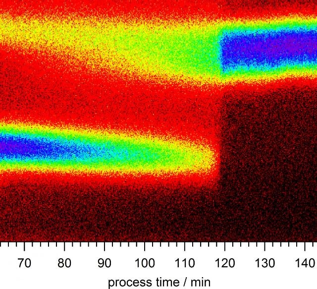 The data (photon energies over time) show defects (lower signal) which disappear after 120 minutes. This happens at the transition from the copper-poor phase to the copper-rich one. (Photo credit: HZB)
A team of researchers from Germany, Israel, and the UK have analyzed the deposition of thin chalcopyrite layers. As these layers were forming during deposition they spotted specific defects developing for the first time, and observed the conditions in which the defects self-healed, with the aid of in-situ X-ray diffraction and fluorescence analysis capabilities of the BESSY II X-ray source at the Helmholtz Zentrum Berlin (HZB). The research outcome provides clues to improve fabrication methods, and has been published in Energy & Environmental Science.
Additional copper helps defects heal
Vapor deposition of thin CIGSe films is a difficult process. Indium, selenium, and gallium are first deposited on the substrate. The deposition of the selenium and copper atoms occurs in a second step. These atoms travel into the In-Ga-Se layer. Miniature CIGSe crystals of chalcopyrite develop there. Copper concentration only reaches the acceptable value during the period of this second step. The previous copper-poor phase is influenced by numerous defects inside the crystal. The defects increasingly vanish when copper and selenium are added. If additional copper and selenium atoms are added after realizing the adequate ratio, then the two elements fail to fit into the existing crystal matrix anymore and deposit themselves as copper and selenium grains on and in the polycrystalline CIGSe layer. This is essentially problematic, as the grains have to be removed at a later stage. However, they have an essential operation in decreasing the defects to near zero, as the current research indicates.
Analyzing growing structures of elements in real time
Dr. Roland Mainz and his colleagues from HZB have examined the alterations to the film structure during deposition using X-ray diffraction at the EDDI beamline of BESSY II, while simultaneously using X-ray fluorescence to evaluate the elemental composition of the thin-film layer as it grew.
The annihilation of the defects takes place very rapidly – just prior to the excess copper-selenium grains being deposited on the surface of the CIGSe film and the film entering the copper-rich phase. So far, we had only understood the copper-rich phase as being important for the growth of the grains. Now we know that it also plays an important role in the elimination of the defects.
Dr Roland Mainz, HZB
Improving vapor deposition processes for high-quality CIGSe films
The paper’s co-author Helena Stange, simulated the power of the different types of defects on the diffraction signal. The in-situ observations fit excellently with the simulations and the results obtained from various imaging methods used to examine the samples in a variety of stages of deposition, by teams at the Max Planck Institute for Solid State Research in Stuttgart, the SuperSTEM Lab in Daresbury, England, and at the Racah Institute, Jerusalem.
A supplementary significant result obtained during deposition is that the temperature represents a comparatively uncritical parameter for defect elimination. As soon as the layer realizes the copper-rich state, it does not make a difference whether the method is executed at 400°C or 530°C. This insight aids to improve the method for depositing onto large surface areas. Other parameters could be improved instead of trying to sustain temperature as homogeneous as possible across the whole surface.
The results have been published in Energy & Environmental Science under the heading: “Annihilation of structural defects in chalcogenide absorber films for high-efficiency solar cells”. The partnership is part of the Helmholtz Virtual Institute of “Microstructure control for thin-film solar cells" that has been funded from 2012 to 2018.