Jul 27 2016
The discovery of the computer chip set the trend for electronic devices to be faster and smaller. However, the flat transistors that are available currently are as small as they can physically be.
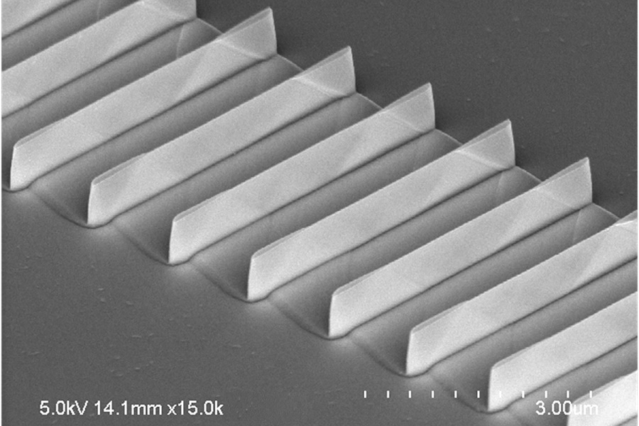 An array fin transistors made by the MacEtch method. The fins are tall and thin, with a higher aspect ratio and smoother sides than other methods can produce. Image Credit: Yi Song
Researchers from the University of Illinois have created a way to etch extremely tall, narrow finFETs, a particular type of transistor capable of developing a tall semiconductor “fin” enabling the current to pass over. A number of issues are addressed with the etching technique during the production of 3D devices, unlike the current method of stacking layers or carving out structures from a semiconductor wafer that is much thicker.
We are exploring the electronic device roadmap beyond silicon. With this technology, we are pushing the limit of the vertical space, so we can put more transistors on a chip and get faster speeds. We are making the structures very tall and smooth, with aspect ratios that are impossible for other existing methods to reach, and using a material with better performance than silicon.
Xiuling Li, Professor, University of Illinois
The results were published by the researchers in the journal Electron Device Letters.
finFETs are typically developed by bombarding a semiconductor wafer with high-energy ion beams. Li stated that several challenges exist in this method. One challenge comes from the fact that the sides of the fins are sloped instead of being straight up and down, causing the fins to resemble more like tiny mountain ranges.
Only the tops of the fins can deliver reliable performance because of this shape. A much complicated issue regarding high-performance applications deals with how damages caused to the semiconductor’s surface by the ion beams can result in current leakage.
Li stated that the Illinois method, known as metal-assisted chemical etching (MacEtch), is a liquid-based technique, which is cost-effective and simpler than using ion beams. A metal template is placed at the surface, and following this a chemical bath etches the areas surrounding the template allowing the sides of the fins to be smooth and vertical.
We use a MacEtch technique that gives a much higher aspect ratio, and the sidewalls are nearly 90 degrees, so we can use the whole volume as the conducting channel. One very tall fin channel can achieve the same conduction as several short fin channels, so we save a lot of area by improving the aspect ratio.
Yi Song, Graduate Student, Unversity of Illinois
The sides need to be smooth as the semiconductor fins must be covered with metals and insulators that touch the tiny wires that connect the transistors on a chip. Song stated that consistent high performance can be obtained only if the interface existing between the semiconductor and the insulator is even and smooth.
Currently, the compound semiconductor indium phosphide with gold is used as the metal template by the researchers. The team is also currently working on developing a MacEtch method that does not require gold, which is incompatible with silicon.
Compound semiconductors are the future beyond silicon, but silicon is still the industry standard. So it is important to make it compatible with silicon and existing manufacturing processes.
Xiuling Li, Professor, University of Illinois
The team stated that the MacEtch technique is capable of being used for a variety of devices that use 3D semiconductor structures, such as LEDs, solar cells, batteries and computing memory.
The National Science Foundation, the International Institute for Carbon-Neutral Energy Research (I2CNER) and Lam Research supported this work. The co-authors of this work include U. of I. postdoctoral researcher Parsian Mohensi (now a professor at the Rochester Institute of Technology) and graduate student Seung Hyun Kim; Jae Cheol Shin, a professor at Yeungnam University in South Korea; Tatumi Ishihara, a professor at I2CNER in Japan; and Ilesanmi Adesida, a U. of I. professor of electrical and computer engineering. Li also is affiliated with the Micro and Nanotechnology Laboratory at the U. of I.