Excellent photovoltaic (PV) components combine several beneficial features, including strong charge carrier mobility and significant optical absorption, all of which are supported by tiny efficient masses. An article in the journal Advanced Functional Materials stated that the golden child of the future generation of solar cells is halide perovskites. The foundation for a perovskite revolution was laid by an advantageous combination of exceptional optical and electrical features combined with cost-effective manufacturing.

Study: Halide Perovskites: Advanced Photovoltaic Materials Empowered by a Unique Bonding Mechanism. Image Credit: Fotografie - Schmidt
The B-X bond, accountable for the charge carriers' significant optical absorbance and small effective masses, governs their optoelectronic capabilities. Particular formulations of perovskite solar cells transform ultraviolet-visible light energy into electrical energy relatively well, suggesting that they could be good hybrid-tandem counterparts for electrode materials like crystalline silicon, which transforms infrared light effectively.
Perovskite's Quantum-Chemical Bond
When the PV features are combined with a quantum-chemical bonds analysis, a distinct situation emerges. Ionic, metallic, and common 2c2e covalent bonds each differ dramatically from the B-X bond. It is best to think of it as metavalent, because adjacent atoms exchange around one p-electron.
ABX3 or halide perovskites have a wide range of applications in optoelectronics, from low-cost, high-performance solar cell modules to lasing devices and light emission. These perovskites have a unique mix of characteristics, including high optical absorbance and substantial charge-carrier mobilities.
The influence of the divalent B cation is commonly credited to the exceptional features of halide perovskites, which permit their promising applications. Materials should enhance their light absorption in the visible spectrum to increase their PV efficiency. They should also have a high electron carrier mobility, which is possible due to their modest effective masses. The structure of the valence and conduction band states involved determines both optical absorbance and effective masses.
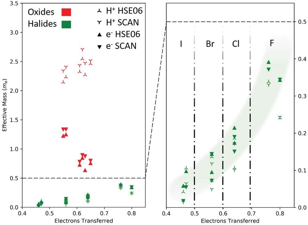
Effective masses of electrons and holes for oxide (red) and halide (green) perovskites. The effective masses for holes (three-pointed stars) and electrons (filled triangles) are computed with the SCAN (symbols pointing down) and HSE06 functional (symbols pointing up) including spin–orbit coupling. The effective masses of the halides are significantly smaller than those of the oxides. It is also noteworthy that for the halide perovskites the effective masses of the electrons and holes increase steadily with increasing relative electron transfer (ET) of the B atom to the surrounding X atoms (a quantity defined in more detail in the text). No such trend is found for the oxide perovskites.
Because oxide and halide perovskites frequently have the same atomic structure but highly distinct optoelectronic capabilities, the nature of the essential electronic properties differ significantly. These differences will be connected to a quantum-chemical bond investigation, which will identify and define the orbitals and bonds accountable for the beneficial PV characteristics.
The effective mass of charge carriers around the Fermi level is a critical parameter for photovoltaics. The curve of the related valence and conductance bands is inversely related to these effective masses.
The hole and effective electron masses in oxide perovskite are much larger than its free electron mass. Low mobilities are a severe drawback for optical applications with such large effective masses. The effective masses of halide perovskites, on the other hand, are substantially smaller.
The halide perovskites hole and electron effective masses show a definite chemical trend. The distinctions between oxide and halide perovskites are due to systematic changes in the Fermi energy's band structure. The conduction bands of halide and perovskites show even more variances. The conduction band lower limit can be found at several locations in reciprocal space. The differing nature of the states in the conduction bands is the reason.
Researchers investigate the link between band structure and chemical bonding to determine why halide perovskites have such low effective masses and significant optical absorption. They use quantum-chemical methods, namely the quantum theory of atoms and molecules, to accomplish this purpose.
The proportional electron transfer, which is calculated by dividing the total electron transfer of halide and oxide perovskites by the oxidation state, is used to compare various substances (nominal ionic charge).
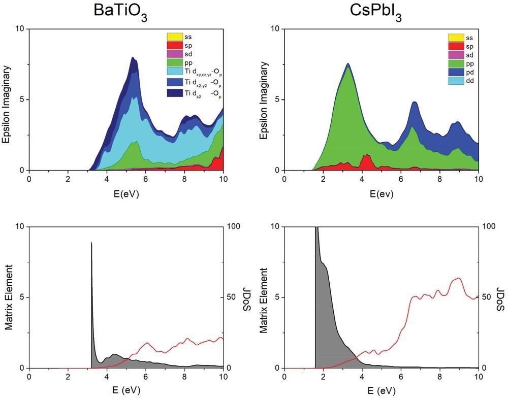
Absorption (epsilon imaginary) for BaTiO3 and CsPbI3 (top), decomposed into the joint density of states (red) and the corresponding average matrix element (shaded area, bottom). In CsPbI3, the absorption maximum is observed at lower energy. It benefits from a large matrix element, dominated by p–p transitions. The optical properties of halide perovskites are thus far superior for PV applications. The joint density of states (JDoS) is in 1 eV−1; the effective matrix element (eV) is defined here as the dielectric constant divided by the JDoS. Data obtained with the SCAN functional.
Excellent Photovoltaic Features
Halide perovskites have a bonding structure that is unique from ionic, metallic, and covalent bonding. The bonding process and the model that explains their optical characteristics are also applicable in the context of the actual hybrid perovskite. The critical bonding features are preserved despite the limited linear and angular distortions.
Many of the excellent photovoltaic features are due to this unusual bonding. As a result, additional materials that use this form of bonding should have comparable appealing qualities.
Another advantage of halide perovskite's metavalent bonding is that it increases the number of atoms in a molecule. It results in a high dielectric constant, which guarantees that charged defect screening is particularly efficient. This lowers defect dispersion and has a positive influence on charge carrier lifetime. It also reduces the connection between electronic motion and lattice distortions and the mass renormalization that occurs as a result.
We can also infer crucial patterns from the quantum-mechanical data that will support the design of future photovoltaic cells. The number of electrons shared and transmitted for the B-X bond is the two most essential chemical bond characteristics for halide perovskites. Both affect optical absorption.
The Peierls distortion grew when the number of electrons exchanged between nearby atoms increased, reducing orbital overlap. This lowers the optical absorbance and raises the bandgap right away. Similarly, as established recently for similar lead chalcogenides, boosting electron transport lowers optical absorbance while increasing bandgap.
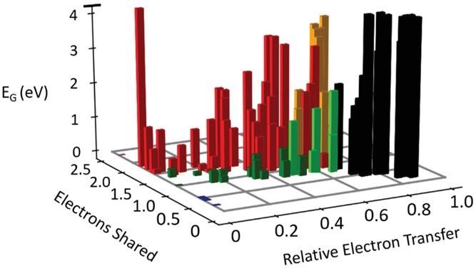
Bandgap as a function of electrons transferred and shared. Different types of bonds are denoted by different colors, i.e., ionic (black), covalent (red), metallic (blue), metavalent (green), halide perovskites (light green), and oxide perovskites (orange). Metavalently bonded systems like PbTe or CsSnI3 are characterized by sharing about one electron between adjacent atoms and modest charge transfer, leading to small bandgaps, strong optical absorption, and small effective masses. The number of electrons shared and transferred can be employed to tune the bandgap and related PV properties.
References
Wuttig, M., et al. (2021). Halide Perovskites: Advanced Photovoltaic Materials Empowered by a Unique Bonding Mechanism. Advanced Functional Materials. First published: 23 October 2021. https://onlinelibrary.wiley.com/doi/10.1002/adfm.202110166
Disclaimer: The views expressed here are those of the author expressed in their private capacity and do not necessarily represent the views of AZoM.com Limited T/A AZoNetwork the owner and operator of this website. This disclaimer forms part of the Terms and conditions of use of this website.