A group of researchers from Spain developed a quasi-3D photonic crystal-based encapsulation for cesium lead halide (CsPbX3) perovskite nanocrystals for use in optoelectronic devices.
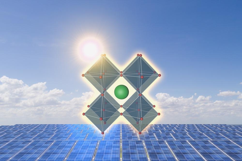
Study: Enhanced Photoluminescence of Cesium Lead Halide Perovskites by Quasi-3D Photonic Crystals. Image Credit: sutadimages/Shutterstock.com
The photonic crystal encapsulation is a combination of 2D-grating and distributed Bragg reflector (DBR) with enhanced photoluminescence than that of a stand-alone CsPbX3 owing to the incorporation of Rayleigh-Wood anomalies and guided modes. Additionally, it provides improved photonic stability and an approach to avoid direct contact with toxic metal halides.
This study is available in the journal Advanced Optical Materials.
CsPbX3 Enclosed in DBR and 2D-diffraction grating for Optoelectronics Devices
CsPbX3 perovskite nanocrystals (NCs) are promising materials for optoelectronic devices such as portable lasers and light sources due to their high photoluminescence quantum yield, narrow emission band, smooth incorporation into inorganic and organic matrices, good environmental stability, scalable synthesis, tunability, and low cost.
However, their potential commercial application is hindered by their toxicity and instability against oxidation and humidity. The solution is to enclose these NCs inside a transparent metal oxide that can enhance their photonic stability without affecting the luminescent properties.
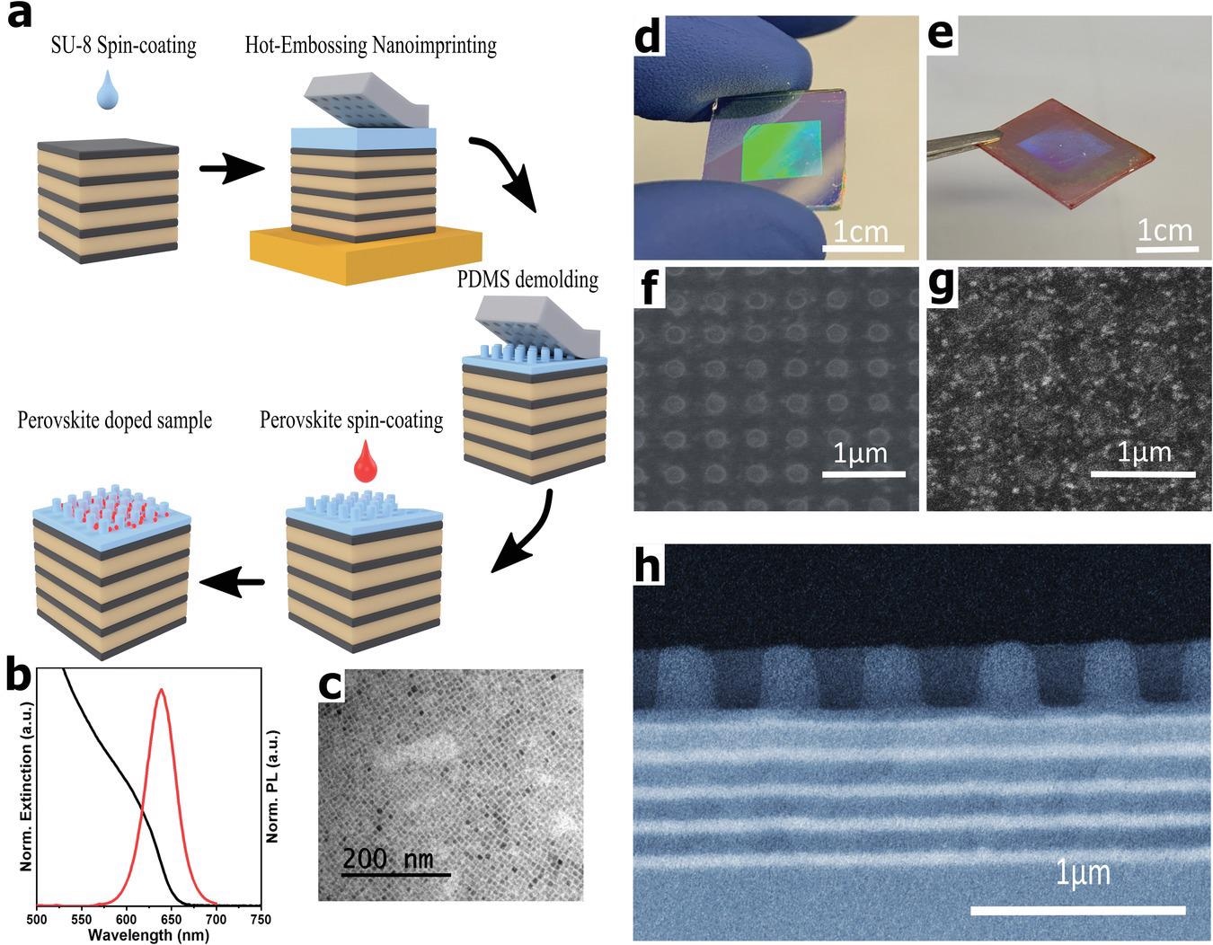
a) Schematic fabrication process of metal halide nanocrystal decorated quasi-3D photonic crystals. b) Absorption (black) and photoluminescence spectra (red) of CsPbBr1I2 nanocubes in hexane. c) TEM Image of CsPbBr1I2 perovskite nanocubes. Photograph of the 1 cm2 quasi-3D crystal under white light illumination d) before and e) after perovskite deposition. Top-view SEM image from the quasi-3D crystal f) before and g) after perovskite deposition. White bright dots around the pillars correspond to perovskite nanocrystals. h) Cross-section SEM image taken from the sample before perovskite deposition with SU-8 pillars on top of a distributed Bragg reflector (DBR) multilayered structure composed of TiO2 (bright) and SiO2 (dark). Image Credit: Carreño, J et al., Optical Materials
Photonic crystals (PCs) regulate the passage of light in a medium by inhibiting the propagation of a specific range of wavelengths that falls in the photonic bandgap. Photonic structures such as 2D-diffraction gratings and DBR inhibit the propagation of lights through absorption and reflection, respectively.
A combination of both photonic systems, where a 2D-grating is placed on the top of a DBR, forms a quasi-3D PC that facilitates resonating in-coupling and out-coupling of electromagnetic waves (EMs), which in turn enhances the performance of the enclosed quantum emitter.
About the Study
In this study, CsPbBr1I2 NCs were used as the quantum emitters, which were synthesized by ultrasonication of Cs2CO3 and PbBr2 in a mixed solvent of octadecene and oleic acid. Furthermore, DBR was fabricated by the deposition of alternating layers of 105 nm silicon oxide (SiO2) and 57 nm titanium oxide (TiO2) on a glass microscope slide using electron beam deposition, where the interface of silica and titania acted as the reflector.
Subsequently, for 2D-diffraction gratings, they used spin coating and nanoimprinting lithography (NIL) of a commercial polymer diluted in a thinner to 6% in weight followed by depositing on the top DBR to form a 140 nm thick photoresist thin film with 2D array pillars. Finally, the CsPbBr1I2 NCs were placed on the top of quasi-3D PC by spin-casting from a suspension solution of NCs and toluene.
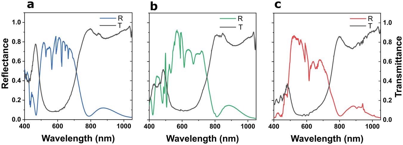
Optical characterization of transmittance (black) and reflectance (colored line) from quasi-3D PhCs for three different pitches. a) 400 nm, b) 500 nm and c) 600 nm under supercontinuum white light illumination. Image Credit: Carreño, J et al., Optical Materials
Observations
Transmission electron microscopy (TEM) and scanning electron microscopy (SEM) image shows cubical NCs with a size range of 10-12 nm on the top of 3D PC and confirmed a 2D-grating consisting of 500 nm pitch, 240 nm wide 2D array pillars on the top of DBR.
The reflectance and transmittance data collected using Fourier-transform infrared spectroscopy (FT-IR) showed the stand-alone 2D-grating had zero reflectance and maximum possible transmittance.
Also, it indicated the presence of Rayleigh-Wood (RW) anomalies in the photoresist film and air. Furthermore, a stand-alone DBR was acting like a dielectric mirror with zero transmittance and maximum reflectance in the photonic bandgap. However, when both DBR and 2D-grating were coupled to form quasi-3D PC, the reflectance maximum peak that was obtained from stand-alone DBR showed a few dips in that bandgap.
Further, ellipsometry measurements showed three major resonances at wavelengths of 585 nm, 532 nm, and 651 nm, which were due to the linear dependence of RW anomalies with lattice parameters (L). Similarly, the broad resonances that did not linearly depend on L were due to guided modes within the DBR. The photoluminescence data shows CsPbBr1I2 perovskite NCs decorating the photonic structure.
Moreover, from the TEM it was evident that the presence of bromide anions in the NCs composition led to a decrease in the degradation ratio of the iodine-containing perovskite, which is highly susceptible to light and humidity. Also, the iodine expulsion during degradation reduced the size of NCs.
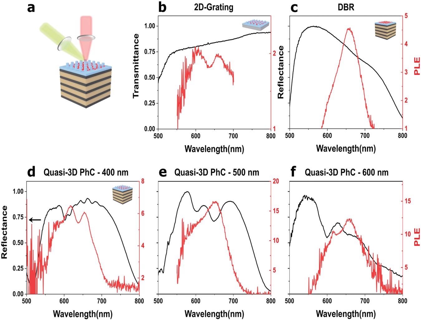
Reflectance or transmittance spectra at normal incidence (black curve, left axis) of the different photonic architectures measured after CsPbBr1I2 NCs deposition versus photoluminescence enhancement (right axis, red curve). a) Sketch of the photoluminescence setup used to pump (green beam) and collect the signal (red beam) normal to the surface. b) Transmittance spectrum (left axis) and PLE spectrum (right axis) of a SU-8 2D-grating on glass. c) Reflectance and PLE spectra of a SU-8 thin film on a DBR. d–f) Reflectance and PLE spectra from three different quasi-3D PhCs with the same DBR and varying the pitch of the 2D-grating: d) 400 nm, e) 500 nm, and f) 600 nm. Image Credit: Carreño, J et al., Optical Materials
Conclusions
The researchers demonstrated a simple and efficient strategy to enhance the quantum emission of CsPbBr1I2 perovskite NCs by spin-casting them on a quasi-3D PC structure consisting of a 2D-diffraction grating on the top of DBR.
The reason for photoluminescence was the resonance of transmitted and reflected wavelengths of light indicated by RW anomalies and guided modes. The final optical performance surpassed the performance of each stand-alone individual component; thus the composite structure is a promising candidate for an enhanced photoluminescence optoelectronic device with improved photostability and non-toxicity for future applications.
Reference
Carreño, J., Passarelli, N., Otero-Martínez, C., Polavarapu, L., Pérez, L. A., Reparaz, J. S., Alonso, M., Mihi, A., Enhanced Photoluminescence of Cesium Lead Halide Perovskites by Quasi-3D Photonic Crystals. Adv. Optical Mater, 2021, 2101324. https://onlinelibrary.wiley.com/doi/full/10.1002/adom.202101324
Disclaimer: The views expressed here are those of the author expressed in their private capacity and do not necessarily represent the views of AZoM.com Limited T/A AZoNetwork the owner and operator of this website. This disclaimer forms part of the Terms and conditions of use of this website.