A new paper has been published in the journal Nanomaterials presenting research into improving the ability of atomic force microscopy (AFM) to image 2D materials at the atomic level. The research has been contributed to by scientists from Hanyang University in Korea and the University of Texas at Austin in the USA.
Study: Accurate Atomic-Scale Imaging of Two-Dimensional Lattices Using Atomic Force Microscopy in Ambient Conditions. Image Credit: sanjaya viraj bandara/Shutterstock.com
Atomic-level Structures
Materials with atomic-level thin layers and van der Waals heterostructures have been extensively studied due to their unique properties and commercial applications for nanophotonics and quantum electronics. These materials are typically synthesized using chemical vapor deposition and mechanical exfoliation techniques, and the material’s properties can be tuned by techniques such as controlling inter-layer twist angles and changing the number of layers.
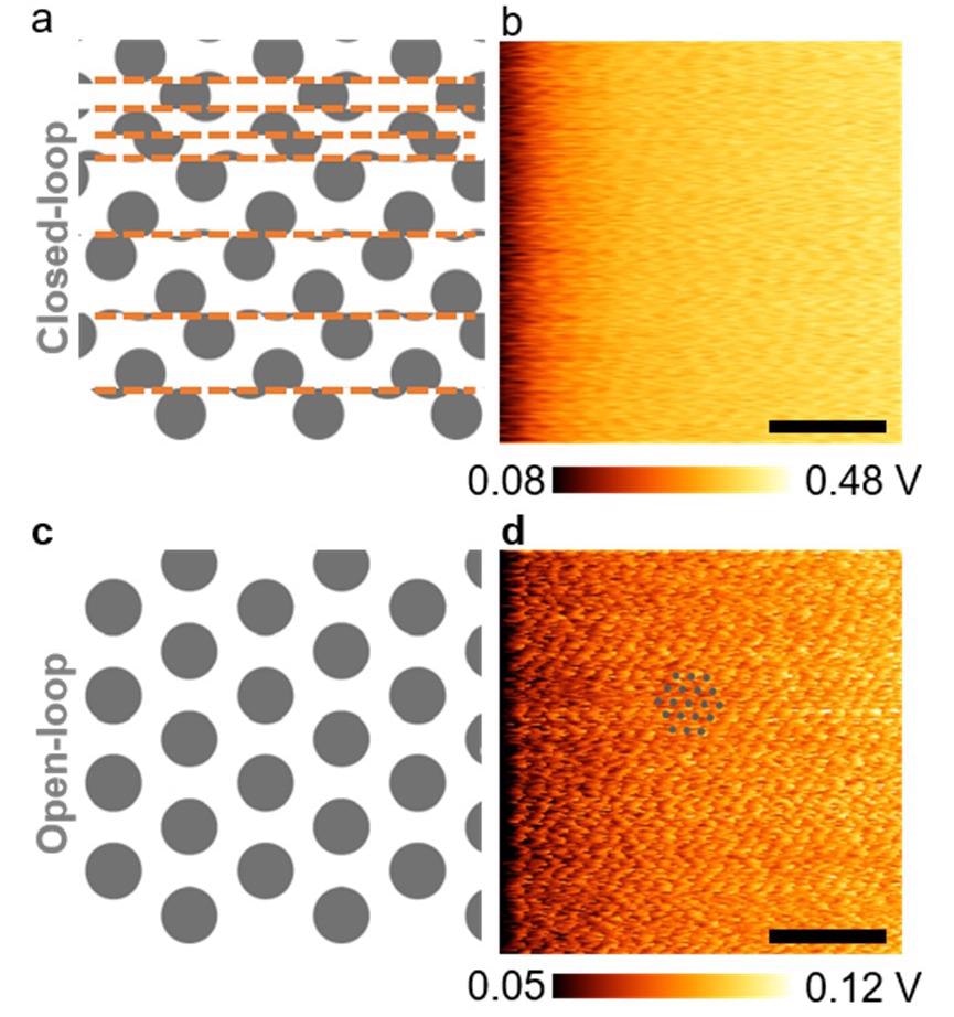
Lateral force microscopy (LFM) raw images obtained with or without engaging the XY closed-loop control in air (color range adjusted). (a) Schematic representation of a jumbled LFM image due to the use of a XY closed-loop control. The orange dashed lines indicate the locations at which the piezo stage was abruptly repositioned due to the XY closed-loop control; (b) LFM image of a MoS2 monolayer obtained with a closed-loop control (calibrated scale bar: 2 nm; scan rate: 21 Hz); (c) schematic illustration of the LFM image of a two-dimensional (2D) lattice expected in the absence of the XY closed-loop control; (d) LFM image of a MoS2 monolayer obtained without a closed-loop control, which revealed a periodic pattern from the atomic lattice (calibrated scale bar: 2 nm; scan rate: 21 Hz). The grey dots are a guide for the eye and correspond to the lattice of rate MoS2. Image Credit: Kim, S et al., Nanoamaterials
Remarkable quantum properties and phases have been discovered by tuning these materials, including quantized exciton states, Hofstadter’s butterfly effect, and unconventional superconductivity. However, there are imperfections that arise during synthesis which can limit the effectiveness of these materials such as bubbles and wrinkles in unstacked van der Waals bilayers. This can cause undesirable spatial variations in disorder and strain in superlattices.
Imaging Atomic-level Structures
Improving techniques for imaging atomic-level structures is a key concern for researchers currently. Non-destructive ultrafast laser imaging methods can image structural properties, stress, and strain at the scale of tens to hundreds of nanometers. Some studies have demonstrated that imaging lattice strain distortion at the atomic level or using scanning probe techniques to control twist angles in the nanoscale heterogeneous structure of materials is possible, but currently, this is challenging.
Various atomic-scale imaging techniques have been developed in recent years, including scanning tunneling microscopy (STM,) transmission electron microscopy (TEM,) atomic force microscopy (AFM,) and lateral force microscopy (LFM,) which is a type of AFM technique. Each method possesses different capabilities and provides different complementary information.
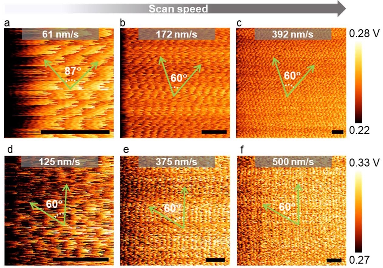
The effect of the scan speed on LFM lattice images (color range adjusted). (a–c) LFM raw data of MoSe2 at various scan speeds (calibrated scale bar: 1 nm); (d–f) LFM raw data of graphene at various scan speeds (scale bar: 1 nm). All green arrows are aligned along the zigzag direction. Image Credit: Kim, S et al., Nanoamaterials
LFM has proven attractive for imaging atomic-level structures due to its advantages over other techniques. Unlike STM and TEM, for instance, it does not require elaborate sample preparation processes which would otherwise damage samples or the need for conducting substrates. The flexibility of this method makes it a versatile tool for the non-destructive characterization of atomic-scale materials under ambient conditions. LFM operates in the contact mode.
Although LFM is a powerful, flexible, and versatile non-destructive imaging technique, several current challenges hinder its widespread adoption. Less-than-optimal parameters and thermal drift can distort images, leading to less accuracy in routine imaging of structures such as 2D atomic lattices. Additionally, if the original image quality is poor or researchers do not follow careful filtering procedures, the authenticity of filtered LFM images can be called into question.
Specialized approaches using symmetrically aligned or tailor-made AFMs, carbon nanotube tips, or specially functionalized tips have been used to produce contact-mode images of 2D lattice structures, but the adoption of these specialized processes is challenging.
The Study
The authors have presented a protocol based on an intimate understanding of feedback loops and parameters such as gain, scan size, and scan rate that influence unfiltered and unflattened LFM images in the presence of drifts. This novel imaging protocol improves the ability of LFM to produce clear, accurate images of 2D atomic lattices.
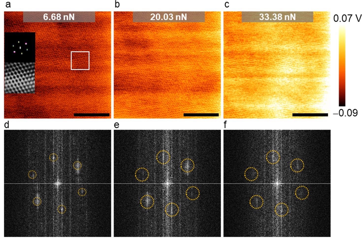
The effect of the load (i.e., setpoint) on LFM lattice images. (a–c) LFM raw data of MoS2 at various loads (calibrated scale bar: 5 nm; frequency: 17.1 Hz). The insets in (a) represent the filtered FFT images of the area enclosed by the white rectangle and its corresponding inverse FFT image; (d–f) corresponding unfiltered FFT images of MoS2. The six FFT spots associated with the hexagonal lattice structure are highlighted with dotted circles. The spots were less noticeable at a load of 33.38 nN, as seen in (f). Image Credit: Kim, S et al., Nanoamaterials
Examples of scan targets used in the study include TMD monolayers and graphene. Selecting the optimal scan parameters decreases geometric distortions in raw LFM images and significantly improves the signal-to-noise ratio. The authors have stated that the protocol allows the accurate identification and interpretation of crystallographic structures in self-folded and torn edges in graphene, improving the determination of crystalline axes present in folded graphene nanoribbons.
The authors have also discussed the effect of substrate roughness and load on the accuracy and sharpness of LFM images of 2D atomic lattice structures. A comprehensive analysis of ninety-nine studies and papers in the current literature was performed by the researchers.
The novel protocol developed by the researchers significantly improves the ability of LFM techniques to produce clear and accurate images of atomic-level structures. It was observed in the study that the optimal scan parameter values vary between laboratories due to their specific drift velocity. The Hertz model was used to estimate the stiffness between AFM tip and Si substrate contact area, which the authors have stated allows other research teams to adapt their protocol.
To summarise, atomic-scale images produced using this novel LFM protocol can be used to identify twist angle variations and local strains to improve the quality of commercially important 2D materials such as MXenes, graphene, perovskites, and van der Waals heterostructures.
Further Reading
Kim, S et al. (2022) Accurate Atomic-Scale Imaging of Two-Dimensional Lattices Using Atomic Force Microscopy in Ambient Conditions Nanomaterials 12(9) 1542 [online] mdpi.com. Available at: https://www.mdpi.com/2079-4991/12/9/1542
Disclaimer: The views expressed here are those of the author expressed in their private capacity and do not necessarily represent the views of AZoM.com Limited T/A AZoNetwork the owner and operator of this website. This disclaimer forms part of the Terms and conditions of use of this website.