Nanoindentation is a measurement technique which is important in measuring Young’s modulus and hardness in thin films and any other situations involving the measurement of limited amounts of material. In most cases, nanoindentation is used to characterize the mechanical properties of films with low dielectric constants (low-k) used in microelectronics.
In such chips, low-k materials are important to separate conducting lines by both mechanical and electrical barriers. The lower the dielectric constant, the better the electrical separation will be. It is difficult to lower the k value, however, using methods such as higher film porosity because these weaken the material itself. The material strength must therefore be balanced against the dielectric constant while designing a microelectronic component. This is where nanoindentation comes into its own in assessing the mechanical robustness of a material with a low dielectric constant.

Figure 1. Measuring the mechanical strength of microelectronic materials is the most common application for nanoindentation.
To conduct a nanoindentation test, films of low-k material are coated on silicon wafers. This, however, introduces the possibility of mistakenly measuring nanoindentation for both the film and the supporting wafer material, which will lead to a falsely high Young’s modulus by the Oliver-Pharr method if this is used alone. This is true even if the indentation is only as deep as a small fraction of the thickness of the film itself. To prevent this, the iNano indentation system uses an autocorrection to compensate for the contribution of the substrate. This will yield a measured Young’s modulus value which is the true one for the material of the film, whatever the wafer may be. This is by calculating the true Young’s modulus (Ef) of the film using the apparent (uncorrected) Young’s modulus (Ea), the depth of indentation produced (h), the film thickness (tf), Young’s modulus for the substrate (Es), and Poisson’s ratio for the substrate material (νs), in the following equation:
Ef=f(Ea,h,tf,Es,νs)
These parameters are usually already known in the case of films of low-k material.
iNano systems measure both Young’s modulus and hardness as continuous functions of the penetration of the indenter by employing a small superimposed oscillation under loading conditions to ensure that maximum penetration depth is not needed (as would otherwise be required to measure these characteristics). This continuous function charting is of great use in the case of thin film testing as it helps to distinguish the relative role of the substrate and the film on the properties measured before and after the correction is made. If the correction is appropriate, the measurements should not vary significantly whatever the depth of the indentation made.
Materials and methods
In this experiment, two samples of low-k materials from a prominent supplier of materials used in advanced electronics, SBA Materials Inc.
Table 1. Summary of low-k samples: physical properties measured by SBA Materials
| Sample ID |
Film thickness (nm) |
Refractive index, n§ |
Dielectric constant, k† |
| A |
196.27 |
1.285 |
2.215 |
| F |
477.51 |
1.283 |
2.169 |
§Measured at a wavelength of 633 nm.
†Measured at 1 MHz.
These were measured with respect to Young’s modulus and hardness using the iNano. A Berkowich indenter was used (as is common) to produce the nanoindentation. Ten indentations were performed on each material sample at room temperature, using the “Dynamic CSR for Thin Films” test modality. The following steps were followed for measurements at each site tested:
- The indenter face was approached and touched the film at a speed of 30 nm/second.
- The strain rate at which the indenter was pressed against the film was 0.2 second, up to the point where it indented 50% of the thickness of the film. The pressure was accompanied by oscillations at 1 nm amplitude and 100 Hz frequency.
- At maximum depth the pressure was kept steady for 1 second (dwell period).
- The force of contact was then decreased to 10% over the next 10 seconds.
- The indenter was kept under constant force for 80 seconds while simultaneously recording its displacement. This was expected to be zero given the unchanging force. However, the true displacement rate measured during this part of the test is not zero because of thermal changes in the material such as contraction-expansion.
- The indenter was removed, and the sample kept in appropriate position for the succeeding test procedure.
Film properties may also be arrived at by the Hay-Crawford model if one knows the thickness of the film and the elasticity of the substrate, and other features, as shown in Table 2.
Table 2. Summary of analytic inputs. (Note: Any of these values may be changed post-test, and the results quickly re-calculated.)
| Input |
Value |
| Drift Correction? |
1 |
| Film Thickness |
196 or 478 |
| Poisson’s Ratio of Substrate |
0.2 |
| Young’s Modulus of Substrate |
170 |
| Poisson’s Ratio of Film |
0.3 |
| Fraction of Film to Start Avg |
0.29 |
| Fraction of Film to End Avg |
0.31 |
| Thin Film (1) or Bulk (0) |
1 |
Results and discussion
Applying oscillation during the loading of the indenter, at 1 nm, 100 Hz, keeps the contact stiff throughout the period of pressing the indenter against the surface of the material. This dynamic stiffness measurement is used in the Oliver-Pharr calculation to obtain the Young’s modulus. The indentation depth standardized to the film thickness is the value on the x-axis and as the depth increases, the modulus becomes larger. This variation is due to the resistance offered to indentation by the stiff silicon of the underlying chip with an E of 170 GPa. Despite and indeed because of the obvious contribution made by the substrate, therefore, these modulus values offer the first move towards the actual result by making the need for correction, and the source of the error, clearer.
The Hay-Crawford model, on the other hand, shows an accurate compensation has been made to correct for the influence of the substrate on the Young’s modulus, by rendering relatively unchanged values in relation to normalized indentation depth. The values obtained in such a case are based on the measured values which have undergone analysis to account for the substrate contribution. Each set of values from different materials is then averaged between 29% and 31% to get one value of the modulus per indentation. The limits of the average are set by the user. As the final step, the mean and the standard deviation are also calculated for each of the ten values so obtained, yielding Ef = 6.48±0.27 and 6.14±0.14 for film A and F respectively.
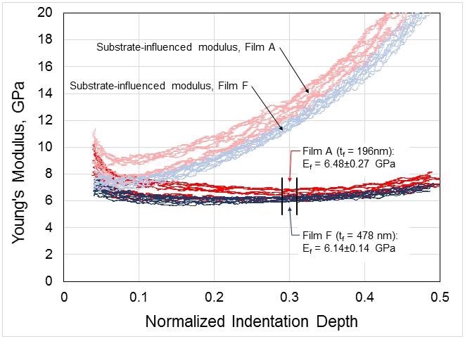
Figure 2. Young’s modulus as a function of indentation depth, normalized by film thickness. Each pink trace represents a single test on Film A, and each light-blue trace represents a single test on Film F. The red and blue traces represent these same physical measurements, respectively, only corrected for substrate influence. Using the corrected traces, film modulus is reported around 30% of the film thickness.
In nanoindentation studies, indentations which go down less than 10% of the film’s thickness are typically taken to be mostly free of any influence from the substrate. This is not true, however, in the case of low-k materials on a substrate which is much stiffer than the test material itself. Thus at 10% indentation, film A has Ea = 8.49 GPa for film A, and Ea = 7.43 GPa for film F, which are 30% and 20% above the actual values for these films. Incorrect results such as these may have a potentially catastrophic impact on the business performance of manufacturers.
Another advantage of the Hay-Crawford model is better accuracy and reproducibility since longer displacements can be allowed before taking measurements, unlike the case when substrate stiffness is an issue. It is more likely that a measurement taken at 50 nm will be correct and repeatable than one taken at only 20 nm because the distorting effect of any experimental artifact will be less likely to be magnified. This includes problems due to a rough and uneven surface, imperfectly smoothed tips, failure of contact detection and vibration of the surroundings. Using this setup, indentation depths may go up to 40% of the thickness of the film without affecting the independence of the results.
Measurement of hardness is not so prone to distortion by substrate stiffness because plastic deformation zones are significantly more limited than elastic deformation zones. When measured using the Oliver-Pharr method, hardness does not increase even as normalized indentation depth increases and no correction is necessary. A single value for each indentation is obtained by averaging data from each point between 29% and 31%, and then mean and standard deviations are also calculated for each value from all the ten tests. This gave H = 1.22±0.06 and H = 1.17±0.03 for film A and film F respectively. The data show that the values are nearly the same when indentation depth approaches 40% of the thickness of the film.
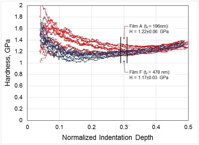
Figure 3. Hardness as a function of indentation depth, normalized by film thickness. Each red trace represents a single test on Film A, and each navy trace represents a single test on Film F. Hardness is relatively insensitive to substrate influence, so no corrective model is needed. Using the original traces, hardness is reported around 30% of the film thickness.
The final data is presented for both samples in Table 2. While E and H values are not very different for both samples, the variation is statistically significant (p< 0.05). Film A is thinner, and its Young’s modulus is somewhat higher, as is the hardness. This is noteworthy because both films were designed to have the same characteristics. The difference is due to the influence of the smaller volume of film A on the microstructure, which in turn affects its mechanical properties, seen as a difference in the dielectric constant between the two materials. Film F is thicker, and the modulus is a little lower, as is consistent with other observations on film thickness and the k-value.
Table 3. Summary of film mechanical properties measured with the iNano
| Sample ID |
N |
Depth range (nm) |
Ef (GPa) |
H (GPa) |
| A |
10 |
56.8 - 60.8 |
6.48±0.27 |
1.22±0.06 |
| F |
10 |
138.6 - 148.2 |
6.14±0.14 |
1.17±0.03 |
Conclusions
The value of nanoindentation is in the relationship between volume and microstructure, and in turn mechanical characteristics of materials. The iNano indentation system uses sophisticated hardware and electronics, as well as offering modern procedures and analyses so that very thin films can also be examined and characterized with more accuracy and with reproducible results. Using this method, two thin films with almost the same low-k value were compared, and the thinner one is associated with a higher Young’s modulus. Such findings are rare with commercial systems especially if thin-film modeling and dynamic indentation during the loading period are not allowed because they are distorted or hidden.
Acknowledgment
Nanomechanics, Inc. gratefully acknowledges SBA Materials, Inc. for providing well-characterized low-k samples.
References
1. Oliver, W.C. and Pharr, G.M., “An Improved Technique for Determining Hardness and Elastic Modulus Using Load and Displacement Sensing Indentation Experiments, Journal of Materials Research 7(6):1564-1583 (1992).
2. Hay, J.L. and Crawford, B., “Measuring Substrate-Independent Modulus of Thin Films, Journal of Materials Research 26(6):727-738 (2011).

This information has been sourced, reviewed and adapted from materials provided by KLA Instruments™.
For more information on this source, please visit KLA Instruments™ .