Accurately characterizing high aspect ratio geometries—such as narrow gaps, deep trenches, and deep holes—is becoming increasingly important across a wide range of technologies and industries. To meet this demand, various metrology techniques are being employed.
Among today’s leading process control tools, 3D optical profiling is gaining traction for its precision and versatility. With its non-destructive non-contact approach and high data accuracy, it’s particularly effective for measuring delicate or sensitive samples.
In this study, deep trenches of varying widths were etched into silicon using reactive ion etching (RIE). While RIE is a standard technique in the industry, optimizing it can be complex.
Factors like critical dimensions, aspect ratio, and feature placement all influence the etch rate—a key parameter in process development. As shown in Figure 1, etch depth can vary depending on the size of the feature. This effect, known as RIE lag or aspect ratio dependent etching (ARDE), is a common and important consideration in microfabrication.
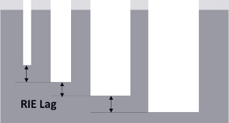
Figure 1. Reactive Ion Etch (RIE) lag is highly influenced by device geometry. Image Credit: KLA Corporation
A common method for characterizing RIE lag involves using a Scanning Electron Microscope (SEM) to analyze the cross-section of the device structure. However, preparing samples for SEM analysis is both destructive and time-consuming.
The Zeta™-20 optical profiler offers a non-destructive alternative by using its proprietary ZDot™ measurement technique to characterize deep trenches with varying widths and aspect ratios. The example discussed in this article demonstrates the RIE lag effect and offers practical guidelines for optimizing fabrication steps during process development.
Deep Trench Measurement Considerations
When measuring deep trenches, it's important to understand the aspect ratio limits of the metrology tool. High aspect ratio structures—particularly those with narrow openings—can be challenging for certain types of profilers to measure accurately.
Choosing the right profiler and measurement technique depends on the specific application and the tool's capabilities. For instance, a stylus profiler typically performs best with samples that have an aspect ratio below 1:1, partly due to the included angle of the stylus tip. White light interferometry (WLI), known for its excellent vertical (z) resolution, may not perform well on samples with high surface roughness.
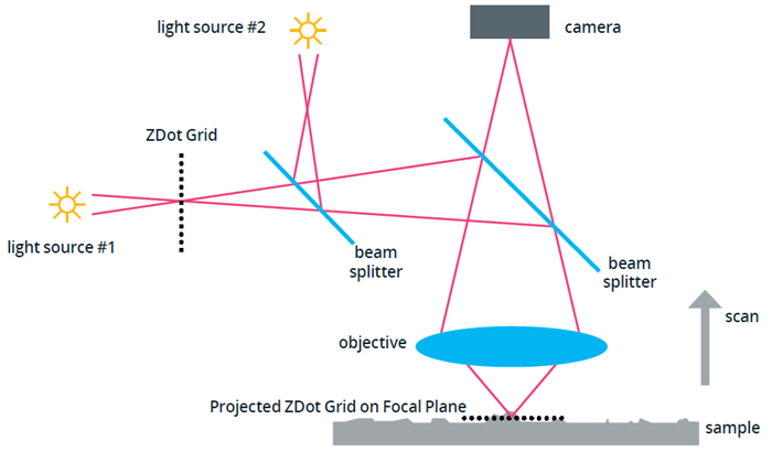
Figure 2. Schematic of the ZDot™ measurement technique. Image Credit: KLA Corporation
The Zeta optical profiler’s unique ZDot technology is featured here to demonstrate its strong performance in deep trench measurement. As illustrated in the schematic in Figure 2, ZDot technology uses a structured illumination technique to enhance the vertical resolution of the objective lens. This improvement is achieved by refining focus across the ZDot grid, which functions like an array of pinholes.
A dedicated light source passes through the ZDot grid, projecting the pattern onto the sample surface. The grid is only in focus when the optics are at the correct vertical (z) position, allowing the system to pinpoint the true height based on the peak optical signal from the grid. The system then identifies the position of best contrast for each pixel to build an accurate 3D topography of the sample.
Simultaneously, a second light source captures a True Color image of the sample, while the first continues scanning the surface topography across varying z positions.
When measuring high aspect ratio trenches, it’s recommended to use low-magnification objectives with smaller numerical apertures (NA). This is because the top surface of the trench acts as an aperture stop, blocking high-angle light from reaching the trench bottom, as illustrated in Figure 3. Only light with a small angle of incidence, relative to the direction perpendicular to the surface, can reach the bottom.
As a result, lower NA objectives (e.g., 0.45 for the 20X objective) experience less blockage of reflected light compared to higher NA objectives (e.g., 0.8 for 50X). Using a lower NA allows for greater light intensity and improves the signal-to-noise ratio during measurement. Additionally, Zeta’s advanced software algorithms further enhance the accuracy of high aspect ratio trench characterization.
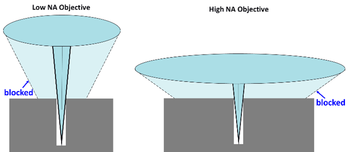
Figure 3. The reflected light in a deep trench is shown for low NA (left) and high NA (right) objectives. Image Credit: KLA Corporation
3D Optical Profiling to Study the RIE Lag Effect
For this study, deep trenches were etched and exposed simultaneously using RIE, then measured with the Zeta-20 3D optical profiler.
The 3D scanning results, shown in Figures 4-6, were all captured using the ZDot technique. Figure 4 presents a top-down True Color image of a 200μm wide trench. The corresponding 3D view in Figure 5 allows for dimensional analysis, with the trench depth measured at 228.09μm.
Figure 6 shows the trench slope and overall shape. Notably, the slope at the trench corners suggests a slower etch rate compared to the trench center.
Figure 4. Top-down True Color image of a 200μm wide trench captured using ZDot technology. Image Credit: KLA Corporation
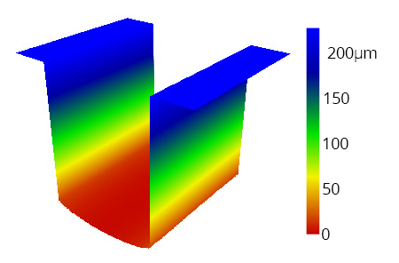
Figure 5. 3D measurement of the trench also captured using ZDot technology, where the color scale represents the Z height. Image Credit: KLA Corporation
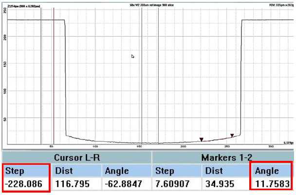
Figure 6. The 2D profiles extracted from the 3D scan reveal the trench geometry, including step height (trench depth) and trench angle. Image Credit: KLA Corporation
Next, narrower etched trenches were examined. For the 100μm and 60μm wide trenches, the measured depths decreased to 217.10μm and 204.92μm, respectively. Figure 7 presents data from a set of 60μm wide trenches. When plotting trench depth as a function of width, a clear trend emerges: narrower trenches result in shallower depths.
This outcome is expected and reflects the well-known RIE lag effect, where narrower features etch more slowly than wider ones. In wider trenches, fluorine radicals can more easily reach the trench bottom, enabling a higher silicon etch rate and deeper trench formation. In contrast, near the trench walls—or in narrower features—the diffusion of fluorine radicals is more restricted, leading to a reduced etch rate.
By adjusting the bias and other process parameters, the RIE etch rate can be tuned to better match the specific pattern being fabricated.
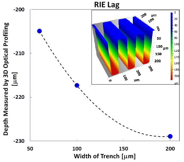
Figure 7. Optical profiling of trench depth as a function of trench width quantifies the effect of RIE Lag, where shallower depths are observed for narrower trenches. The inset shows the 60μm wide trenches. Image Credit: KLA Corporation
Lastly, we compared the Zeta optical profiler results with SEM measurements taken from the same wafer and found excellent correlation, as shown in Figure 8. The slight offset between the SEM and optical profiler results can be attributed to differences in measurement location on the wafer. These correlation results support the use of Zeta measurements as a complementary tool alongside SEM.
The Zeta 3D optical profiler proves to be a reliable solution for characterizing deep trenches and serves effectively as a quality control tool for monitoring trench geometries, including the RIE lag effect, throughout the microfabrication process.
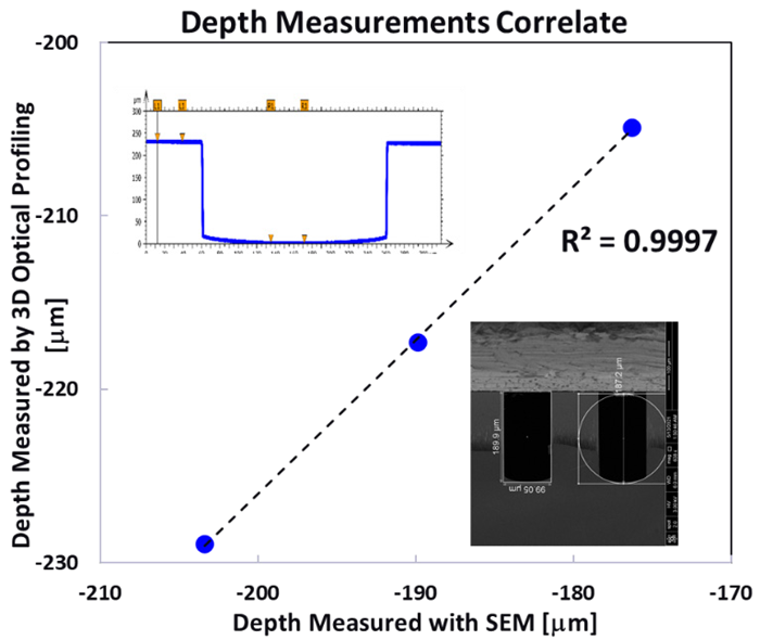
Figure 8. Correlation of the Zeta optical profiler result (profile shown at top left) and SEM result (profile shown at lower right). Image Credit: KLA Corporation
High Aspect Ratio Trench Measurement
An additional assessment was conducted on even narrower trenches with higher aspect ratios, ranging from 5:1 to 15:1. As discussed earlier, a 20X objective with a smaller numerical aperture was used for this part of the study to ensure optimal measurement performance.
Figure 9 shows a top-down image of three trench sets with widths of 40μm, 20μm, and 10μm. The corresponding measured depths, shown in Figure 10, ranged from 190.0μm for the 40μm wide trenches to 152.2μm for the 10μm wide trenches.
As expected, the wider trenches were deeper than the narrower ones. The depth difference between adjacent trench widths was approximately 20μm, further confirming the RIE lag effect observed in earlier measurements.
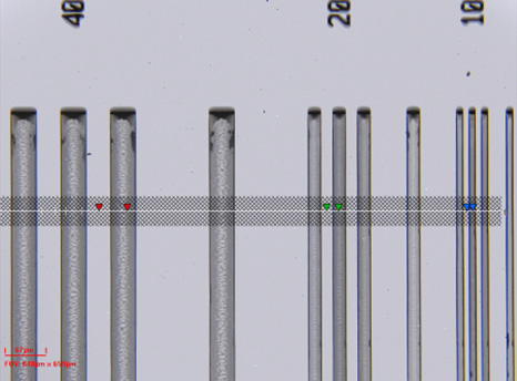
Figure 9. A top-down Zeta True Color image of three sets of high aspect ratio trenches, with nominal widths of 40μm, 20μm and 10μm. Image Credit: KLA Corporation
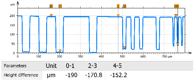
Figure 10. 2D profile taken from the 3D scan shows high aspect ratio trench depth measurements for the three different trench widths. Image Credit: KLA Corporation
Additional Characterization of Trench Topography
Comprehensive characterization of deep trenches is essential, as surface roughness and the shape of the trench edges can significantly impact device performance. A closer view of the 200μm wide trench bottom, shown in Figure 11, reveals both the surface profile and the curvature at the base. This curved shape is characteristic of the RIE process, where the etch rate tends to slow near the edges.
To better understand these variations, it’s important to quantify the curvature across different trenches. Using the definition provided in anISO 12181, the radius of curvature (shown in Figure 12) was calculated to be 372.1μm.
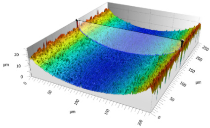
Figure 11. A zoomed-in area of the 3D scan illustrates the curvature and roughness of the bottom of the trench; the 2D scan position is indicated. Image Credit: KLA Corporation
Surface roughness of the etched silicon is another critical parameter in process development. The Zeta tool’s unique feature detection capability allows for automatic identification of areas of interest within the field of view (FOV), including collective measurement of trench bottom roughness.
These measurements are driven by customizable threshold settings, such as height, pixel intensity, RGB values, size, and shape.
In this case, the regions of interest are the center areas of the trench bottoms. Size and depth were used as threshold criteria, allowing the software to automatically detect and highlight the middle region, as shown in Figure 13. Height differences were calculated relative to a user-defined reference area located in the upper left of the image.
Within the FOV, three trench centers were successfully identified. The software then automatically generated roughness statistics—including Sa, Sq, Spv, and Sz—as well as height difference values in the results report.
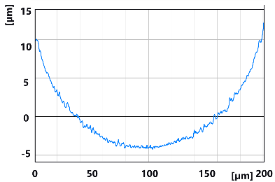
Figure 12. A 2D profile from the 3D scan in Figure 11 is used to calculate the radius of curvature at the trench bottom as 372.1μm. Image Credit: KLA Corporation
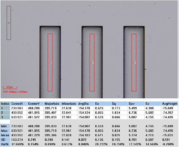
Figure 13. The Zeta software automatically detects the measurement areas based on user-defined threshold settings. The depth and roughness measurements are displayed in the output report. Image Credit: KLA Corporation
All analysis settings can be saved as part of a measurement recipe and reused across multiple locations during a sequence. In sequence mode, the XY stage automatically moves to the next measurement point once the previous scan is complete. A final report is then generated, compiling results from all sequence measurements.
As this process is fully automated, the Zeta software is well-suited for characterizing trench arrays and producing measurement statistics for entire wafers—or multiple wafers—in a production environment.
Conclusion
The Zeta optical profilers from KLA Instruments, featuring patented ZDot™ technology, provide precise, non-destructive measurement of deep trenches with widths ranging from 10μm to 200μm and beyond. This study demonstrated high-performance, automated measurements of high aspect ratio trenches and showed excellent correlation between optical profiler and SEM results.
In summary, the Zeta optical profiler offers a reliable, efficient solution for characterizing deep trench geometries and quantifying the RIE lag effect during high aspect ratio device microfabrication.

This information has been sourced, reviewed and adapted from materials provided by KLA Instruments.
For more information on this source, please visit KLA Instruments.