Failure analysis typically begins with identifying a region of interest (ROI) on a sample for detailed examination using tools such as a Scanning Electron Microscope (SEM), Focused Ion Beam (FIB), or Atomic Force Microscope (AFM).
One common method involves using a hand-held scribe to mark the sample while observing it under an optical microscope. This approach can work well when the feature in question is large and visually distinct from its surroundings.
However, marking small features presents a unique challenge, especially when the ROI resembles other areas on the sample and requires higher optical magnification to identify accurately.
As magnification increases, the working distance (the space between the objective lens and the sample) decreases significantly. This reduced clearance can make it difficult, or even impossible, to bring a conventional hand-held scribe close enough to the ROI.
There's also a risk of accidentally damaging the area during the process. As a result, the scribe mark may end up too far from the ROI, complicating its location during subsequent SEM or FIB analysis.
Another consideration is that SEM and FIB systems cannot image through certain layers, such as photoresist or other organic materials, which are transparent under an optical microscope. This makes accurate ROI marking even more critical.
The KLA Instruments™ Zeta™ Series 3D optical profilers address these challenges with an integrated diamond scribe capability. These systems utilize a precision diamond-tipped scribe mounted directly within the microscope, allowing for easy and accurate marking of the ROI.
The scribe is aligned and fixed on the same turret that holds the microscope’s objective lenses. Because the turret is motorized and computer-controlled, users can quickly and precisely place scribe marks near the ROI with minimal risk.
Figure 1 shows a close-up of the diamond scribe mounted on the turret.
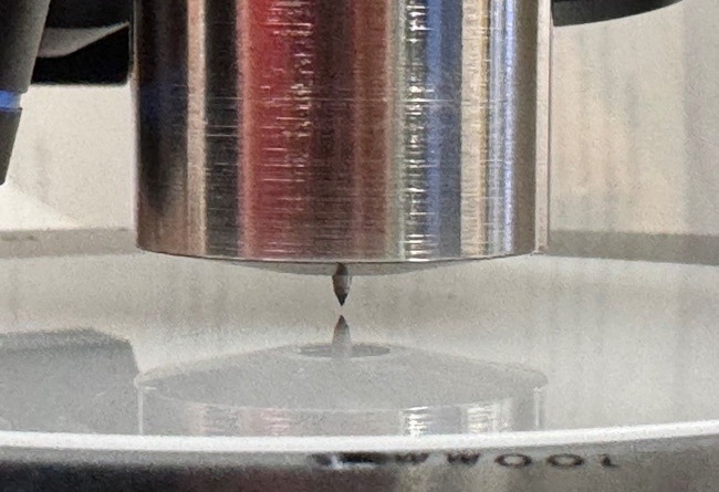
Figure 1. Diamond scribe mounted in the Zeta-20 objective turret. The scribe is in the middle of the holder, pointing down toward the wafer below. Image Credit: KLA Corporation
Diamond Scribe Applications
The Zeta diamond scribe has been used in a variety of applications, including marking places for FIB sample preparation, SEM analysis, and AFM imaging. It can be used in industrial and research laboratory settings in applications such as:
- Failure Analysis
- Material Analysis
- Defect localization
- Semiconductor
- Microscribe & circuit cleave
- Mark for FIB
- Mark defect located under the photoresist for FIB-SEM
- Microelectronics
- Bumps, pads, and copper pillars on various wafer types
- Defect Inspection
- Mark sub-micron to large-sized features
- Mark mask and device defects located by Automated Optical Inspection (AOI)
- Optical
- Packaging
- Cosmetic and Appearance
- Scratches
- Regions of different colors
- Regions of different textures
The integrated diamond scribe is designed to work with materials across a wide range of hardness levels. Users can choose from three diamond tip geometries (2 µm, 5 µm, and 10 µm) to match the specific requirements of their samples. Combined with programmable force control, this flexibility enables precise scribing on both soft and hard materials.
This capability proves valuable not only in failure analysis but also in process development—whether for creating new devices or refining existing components. A wide variety of analytical, optical, and metrology techniques can benefit from the integrated scribe, including AFM, Auger, ellipsometry, ESCA, FIB, FTIR, Raman, SEM, and more.
Diamond Scribe Example Usage
Figure 2 shows diamond scribe markings on aluminum, glass, and silicon—three materials with significantly different hardness levels. The force applied by the diamond scribe is adjustable, and in this example, the applied load increases from the bottom to the top of each column, as well as from left to right across the three columns.
Despite these variations in hardness, the integrated diamond scribe produced clearly defined marks on all three materials. It is also capable of marking other materials with hardness values ranging from softer than aluminum to harder than silicon.
Multiple scribe patterns come pre-programmed to support a variety of application needs. The pattern shown in Figure 2, for instance, is ideal for tuning the diamond scribe’s force settings.
Figure 3 displays a cross pattern designed to frame and point directly to the ROI, with adjustable line lengths to control the distance between the ROI and the ends of each line. Figure 4 shows a staggered pattern, which can be particularly helpful for quickly identifying the orientation and location of a ROI that may be difficult to visualize.
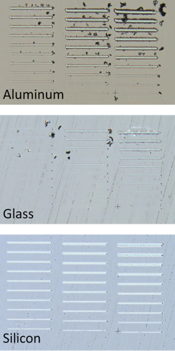
Figure 2. The diamond scribe can mark materials over a wide range of hardness values, including aluminum (top), glass (center) and silicon (bottom). Image Credit: KLA Corporation
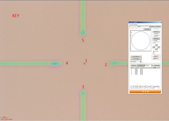
Figure 3. Patterned cross; the Region of Interest (ROI) is located next to the number 1 at the center of the cross. Image Credit: KLA Corporation
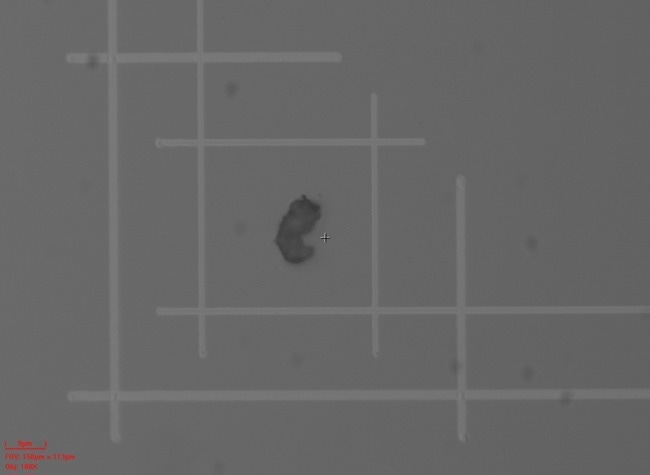
Figure 4. A staggered pattern improves the ability to locate the ROI in the analysis tool after FIB-preparation of the sample. Image Credit: KLA Corporation
Synergy of the Diamond Scribe with Automated Defect Detection
The diamond scribe capability works in tandem with the Automated Optical Inspection (AOI) functionality of the Zeta Series systems. AOI is a powerful tool for scanning samples to detect and characterize defects based on their location and size. It is particularly useful for:
- Identifying isolated defects that are difficult to locate,
- Compiling statistical distributions of defect sizes when multiple defects are present, and
- Conducting Defect Review.
During Defect Review, users can optically profile a defect’s topography, use the integrated diamond scribe to mark its precise location for further analysis, and export a KLARF file containing defect coordinates. This data can then be used in downstream processes such as pick-and-place operations or additional inspection workflows.
Figure 5 shows two instances from a large collection of fault topographies that can be discovered using AOI.
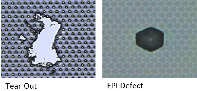
Figure 5. Examples of defects that can be located using the Zeta AOI defect detection application. Image Credit: KLA Corporation
The AOI application generates and sorts lists of all discovered flaws (which can number in the hundreds or more). Figure 6 shows how a specific fault from the defect list was picked and then positioned in the field of view of the low magnification objective lens, ready for additional optical investigation.
A higher magnification lens is then selected and installed using the automated turret. Figure 7 shows measurements of defect height and lateral dimension at increased optical magnifications using ZDot™ technology.
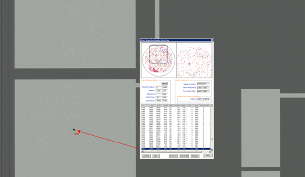
Figure 6. Defect Traceback of the Zeta AOI analysis capability. Image Credit: KLA Corporation
At this point, the benefits of diamond scribing, ZDot characterization, and AOI fault identification become clear. The diamond scribe is switched into position, and fiducial marks are scribed on the sample.
Additional defects can be chosen from the AOI defect list, assessed for vertical and horizontal geometries, and noted for subsequent analytical investigation in a similar manner.
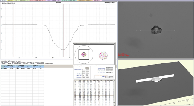
Figure 7. High-resolution imaging of a defect located using AOI. Image Credit: KLA Corporation
Conclusion
The Zeta™ Series 3D optical profilers use ZDot™ imaging technology to provide versatile metrology tools for analyzing a wide range of samples. The accessible inbuilt diamond scribe can precisely indicate the position of a ROI on both hard and soft materials for future investigation.
Combining the integrated diamond scribe with automated optical inspection and defect evaluation creates a powerful tool for connecting optical metrology to later analytical measurements.
This information has been sourced, reviewed and adapted from materials provided by KLA Instruments.
For more information on this source, please visit KLA Instruments.