Manufacturing Printed Circuit Boards and Printed Wiring Boards
A printed circuit board (PCB) is a core unit of an electronic device with electronic parts mounted on a circuit board. The electronic parts conduct appropriate amounts of current or electric signals through the circuit pattern to make the electronic device operate. In comparison, a printed wiring board (PWB) is a board with electronic parts in a circuit pattern that has not been mounted.
The PCB manufacturing process starts with a piece of copper foil. The foil is pasted on the plate of an insulator made of epoxy resin and glass. Then an agent called resist is printed on the copper. Next, the copper portion surrounding the resist is removed using an agent, forming a circuit on a board.
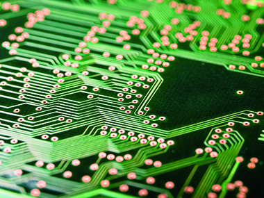
Recently, the use of multilayer circuit boards is becoming more common. This type of circuit board provides multi-functional electronic control with multiple layers of circuit boards.
An image of a multilayer circuit board.
Even though PCBs have controlled electronic devices for a long time, electronic device functionality has considerably improved in recent years. As a result, quality and performance improvements are expected.
Take this example: as the functions of smartphones, tablets, and wearables increase, mounting parts in high density on a PCB is becoming essential. Hybrid electric and fully electric vehicles are also rising in popularity, leading to more expectations for circuit boards to precisely conduct large amounts of current to drive these vehicles.
Products are also emerging for the automated driving of vehicles, such as an automotive millimeter-wave radar. This product produces radar waves from the circuit board. Innovations like this are drawing attention to new uses of circuit boards.
One of the technologies that supports these new electronic devices is the higher precision of circuit shapes. The circuit must be formed precisely to conduct the signal or current. Otherwise, the conduction will fail, which may prevent an electronic device from working properly.
During the manufacturing process of PWBs, the shape of circuits is measured using an automated device that inspects the boards’ appearance. However, with large numbers of circuit boards to inspect, inspection time is limited, so automation may result in overlooked defects.
Therefore, a microscopic inspection is required to analyze circuit shapes precisely. Some inspectors may turn to conventional digital microscopes to perform this task. However, these digital microscopes present three main challenges for inspectors.
Challenges of Measuring Circuit Shape with a Conventional Digital Microscope
Low image resolution
Conventional digital microscopes usually provide one lens with a broad magnification range using zoom. The problem is, image resolution decreases as magnification increases. This leads to a blurred image, making it difficult to measure the circuit shape.
Often, inspectors must see multiple types of circuit shapes on the same printed wiring board. However, it is impossible to obtain a clear image of all circuit shapes using a conventional digital microscope.
Complex lens replacement
While conventional digital microscopes have high-magnification lenses, many models only include one lens. This means that any time a user changes the magnification, the current lens must be replaced. This makes measuring the circuit shape a time-consuming process because users must find the circuit focus position again.
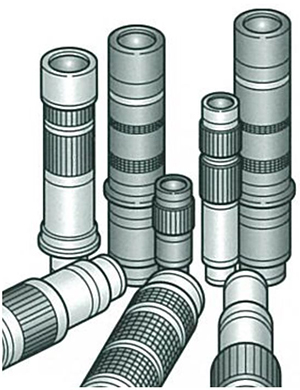
Image Credit: Evident Corporation - Industrial Microscopy
Unreliable measurement values
Many digital microscope manufacturers do not guarantee measurement accuracy and precision. Without a guarantee of the circuit shape measurement value, the data is unreliable.
Benefits of Measuring Circuit Shape with the DSX1000 Digital Microscope
High-resolution objective lenses achieve clear images
The DSX1000 digital microscope comes with high-resolution objective lenses. Zooming in to a high magnification leads to a high-resolution image, which users cannot attain with a conventional digital microscope. The high-resolution images enable users to precisely measure the circuit shapes of PWBs.
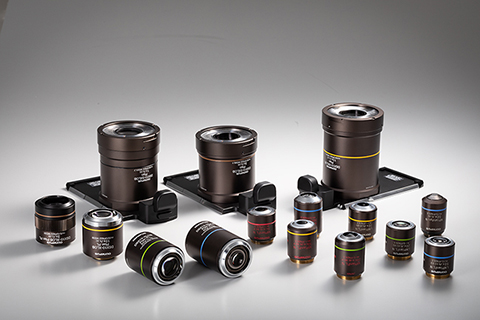
DSX1000 objective lenses. Image Credit: Evident Corporation - Industrial Microscopy
Quick-change lenses offer flexibility
Changing magnification with quick-change lenses is a swift and easy process. Users can switch the magnification from low to high (or vice versa) without the need to search for the focus position again. With a wide range of easy-to-change lenses available, users can measure using the ideal objective for the circuit shape size.
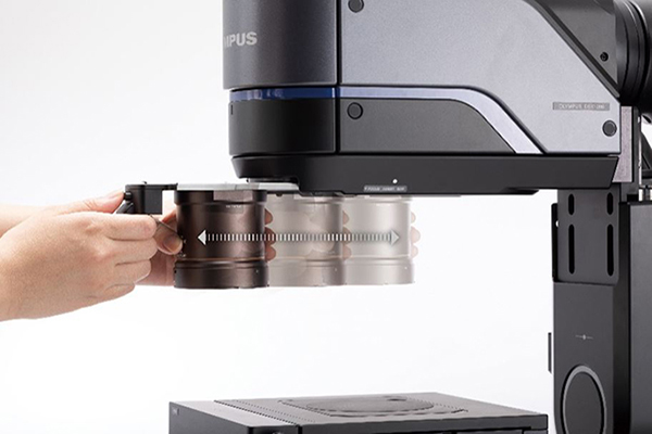
Quick-change lenses.
Quick-change lenses offer flexibility
Changing magnification with quick-change lenses is a swift and easy process. Users can switch the magnification from low to high (or vice versa) without the need to search for the focus position again. With a wide range of easy-to-change lenses available, users can measure using the ideal objective for the circuit shape size.
Image Credit: Evident Corporation - Industrial Microscopy
Example Images
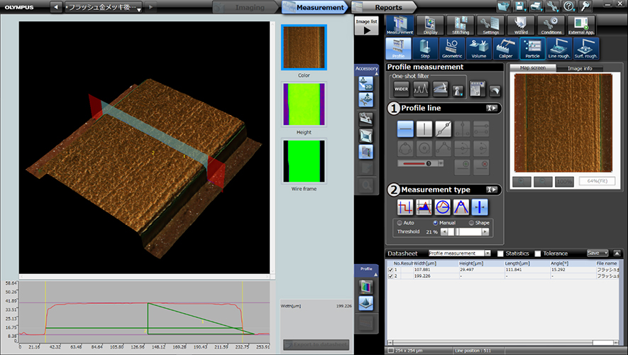
The circuit shape of a printed wiring board captured using the DSX1000.

This information has been sourced, reviewed and adapted from materials provided by Evident Corporation - Industrial Microscopy.
For more information on this source, please visit Evident Corporation - Industrial Microscopy.