In this interview, Dr. Daniel Goran, Sr. Product Manager for EBSD at Bruker Nano Analytics talks to AZoM about the new and augmented on-axis TKD solution in the SEM.
Please introduce yourself to our readers and tell us about your role at Bruker Nano Analytics.
I’m an “incurable” engineer and a space enthusiast. I joined Bruker in 2009 as EBSD Application Scientist and since 2012 I’ve been responsible for the EBSD product, working on product development, and new applications development with multiple groups worldwide.
The SEM Transmission Kikuchi Diffraction (TKD) method allows the characterization of nanostructures. Please can you give a brief explanation of TKD, its history and how it has improved the field of nanomaterials?
Transmission Kikuchi Diffraction (TKD) in a Scanning Electron Microscope (SEM) was first proposed in 2012 and then quickly became an established technique due to its much better spatial resolution as compared to Electron BackScatter Diffraction (EBSD). TKD, a.k.a. t-EBSD (transmission-EBSD) requires an electron transparent sample placed horizontally or slightly tilted underneath the electron beam so the EBSD camera captures a transmitted Kikuchi pattern from below the sample plane.
The initial sample-detector configuration a.k.a off-axis TKD (see Fig.1.b)) was optimized a few years later by the introduction of on- axis TKD (see Fig.1.c)), resulting in major improvements in signal yield and reduced gnomonic projection distortions in the patterns. To achieve this, we modified the standard, vertical EBSD screen (see Fig.1.a)) to resemble a STEM detector featuring a plane mirror inclined at 45 degrees placed underneath a horizontal screen/scintillator (see Figure 1.c)).
The new and improved TKD detector head has been commercially available since 2015 under the name OPTIMUS TKD. Its introduction has led to significant gains in spatial resolution, data acquisition speed and data integrity for SEM-based TKD. OPTIMUS has expanded the range of applications for TKD by enabling characterization of nanomaterials that previously required a Transmission Electron Microscope (TEM). OPTIMUS TKD has also been successfully used to characterize electron beam sensitive and soft materials [11], advancing research in low energy transmission electron microscopy.
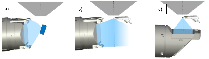
Figure 1. Sample-detector geometry for: EBSD a), conventional TKD b) and on-axis TKD c). Image Credit: Bruker Nano Analytics
What is the OPTIMUS 2 and how does it expand the applications field of TKD?
OPTIMUS 2 is the successor of OPTIMUS TKD and is the result of a collaboration project with a team of researchers from DTU Nanolab in Copenhagen, Denmark. OPTIMUS 2 brings new imaging capabilities that improve the spatial resolution during mapping and boost data quality and integrity. These advances allow On-Axis TKD measurements during in-situ heating or tensile experiments and enable orientation mapping using the Ultra High Resolution mode of certain SEMs with immersion lenses, a feat that was impossible until now.
What are the key new features of the OPTIMUS 2? How has it improved compared to the original OPTIMUS TKD detector head?
There are four key new features:
- OPTIMUS Vue screen with a Si diode at its center for Bright Field (BF)-like imaging
- Advanced alloys to reduce interference with e-beam
- Additional new thin film in the screen active layer for improved signal quality
- Optimized screen frame design for an improved user experience
OPTIMUS Vue is the most important new feature as it results in major specification improvements, and enables powerful new software features. Some of the benefits include:
- Best spatial resolution possible by providing perfect conditions for optimizing beam focus and astigmatism settings before acquiring a TKD map
- Near real-time visualization of electron transparent samples during in-situ experiments in the SEM using the new ESPRIT TRM feature for Time Resolved Measurements
- Improved data integrity: high contrast BF-like images are ideal input-data into the image correlation algorithms used by the ESPRIT Drift Correction feature. This benefit is particularly important for TKD maps where beam and/or sample drift of just a few tens of nanometers can result in visible artifacts in the map unless drift correction has a high degree of accuracy.
- Productivity boost: BF-like images can now be binarized using the new ESPRIT MaxYield feature and used as masks for efficient mapping of dispersed samples like grids containing nanoparticles or nanorods
- Convenience, efficiency and success during the calibration procedure of the new ESPRIT FIL-TKD (Full Immersion Lens TKD) feature enabling, for the first time ever, TKD mapping using the immersion lens mode, a.k.a. UHR-mode, of certain electron columns
Please outline the specifications of the OPTIMUS 2.
- Effective spatial resolution down to 1.5 nm (dependent on SEM type, vacuum quality and room environment, e.g. vibrations, acoustics, etc.)
- Mapping speed: up to 630 pps
- 3 + 1 Si diodes for DF-like and BF-like imaging at up to 125,000 pixels/s
- Fast & Automatic ARGUS signal optimization in ESPRIT 2 software
- Low probe current operation (less than 2 nA even for high-speed mapping)
- Operating beam voltages: 5 kV – 30 kV
- User replaceable phosphor screens
- High performance phosphor screen optimized for maximum signal efficiency and reduced beam interference
- Seamless combination with Hysitron PicoIndenter PI89 for analysis of electron transparent samples during in-situ tensile testing
What technology advances does this development bring?
OPTIMUS 2 combined with the new SW features mentioned above, will have a significant impact in major industries like semiconductor and energy storage as well as in academic research on nanomaterials and nanostructures. By pushing the resolution limit of orientation mapping below 2nm, OPTIMUS 2 will enable a larger number of scientists to perform analyses in an SEM that until now were limited to TEMs. Furthermore, certain types of in-situ experiments have requirements that cannot be met by TEMs, e.g. space, vacuum levels, etc. OPTIMUS 2 will enable “low-kV TEM” analyses during such dynamic experiments which would otherwise not be possible. These are many ways in which OPTIMUS 2 will help advance technology and fundamental research. I am convinced that with the help of the scientific community we will find new applications for on-axis TKD technique and new ways to improve it even further in the future.
How can accurate quantitative EDS analysis be carried out in combination with Bruker’s XFlash FlatQuadEDS detector?
Cliff-Lorimer-factor and Zeta-factor quantification methods designed for EDS on TEM can be used to accurately quantify EDS spectra acquired from electron transparent samples in the SEM. Using the XFlash FlatQUAD EDS detector with its unique on-axis positioning, we can acquire hyperspectral maps at speeds far superior to those achieved with a standard EDS detector, even if the latter has a very large active area.
What are the benefits of combining EDS and TKD measurements?
Combined EDS and TKD measurements are ideal for characterizing little-known samples containing multiple crystallographic phases, e.g. precipitates and/or inclusions. The combined dataset can be used for offline phase identification and reanalysis with great efficiency gains enabled by ESPRIT 2’s capability of indexing up to 60,000 patterns/second. The chemical information can also be used to separate phases that are chemically different but crystallographically similar, e.g. metals & alloys with an FCC structure. Furthermore, the EDS signal could be used to get an insight into those regions of a high entropy alloy which may exhibit semiamorphous or amorphous properties from which it would be impossible to extract information using TKD alone.
OPTIMUS 2 has built-in ARGUS imaging features. How does this imaging, the Si diodes used, the ESPIRIT 2 software and OPTIMUS-VUE screen combine to provide unique imaging capabilities?
Like its predecessor, the OPTIMUS 2 detector head features built-in ARGUS imaging capabilities. With three silicon diodes at the front edge of the phosphor screen and a new silicon diode at the screen center, OPTIMUS 2 provides:
- Dark Field (DF)-like false color imaging
- Bright Field (BF)-like imaging while in TKD mapping position
- Imaging at speeds of up to 125,000 pixels/second
- Fully automatic signal optimization to create images with unequalled quality and detail
The new BF-like imaging capability is particularly useful for drift correction during mapping as well as for near real-time visualization of samples during dynamic experiments like in-situ tensile testing, heating and electrical biasing of electron transparent samples.
Tell us about the new ESPIRIT TRM (Time Resolved Measurements) feature.
ESPRIT TRM feature is the perfect complement of the new BF-like imaging capability brought by OPTIMUS 2. It is intended specifically for observing all important microstructural changes happening during very dynamic experiments like in-situ heating and electrical biasing. The acquisition and saving of BF-like images and TKD maps is automatic and repeated for a user defined duration of time, e.g. duration of a specific step or even the entire experiment.
How does the OPTIMUS 2 combine with Bruker’s PI89 Hysitron PicoIndenter?
The Hysitron PicoIndenter PI89 was designed for a seamless integration with e-Flash EBSD detectors retrofitted with the OPTIMUS 2 head during in-situ experiments. Tensile testing of electron transparent samples using the PI89 can now be observed in close to real-time thanks to OPTIMUS 2 and the new ESPRIT TRM feature.
What applications can the OPTIMUS 2 and its superior nanomaterial characterization be used for?
Considering there is a minimum number of pixels needed to resolve a microstructural feature and that we can achieve an effective spatial resolution down to 1.5 nm, OPTIMUS 2 can be used to characterize nanomaterials and nanostructures with crystals as small as 5 nm. OPTIMUS 2 and On-Axis TKD can practically be applied to all fields of research and development, industrial or academic, working with such crystalline nanomaterials regardless of their form: bulk, particles, rods, wires, sheets/2D, etc.
Does the OPTIMUS 2 compare with anything else on the market today?
Bruker’s unique on-axis TKD solution of which OPTIMUS 2 is a major component, has significant advantages compared to conventional off-axis TKD based products. Advantages include but are not limited to spatial resolution, probe current requirements, data quality and integrity as well as capabilities like BF-like imaging and orientation mapping in “immersion mode” of certain SEMs. These features are not available with any other EBSD/TKD system.
What do you see in the future of TKD and SEM in nanomaterial characterization and what part will Bruker play in this?
Quantitative nanomaterials characterization in the SEM has a very bright future with plenty of opportunities for technology and application development. Except for those applications requiring sub-nanometer resolution for which a TEM will still be needed, any other application will eventually be SEM based for two major reasons: economics and a very flexible experimental platform. With basic capabilities like crystallographic and elemental mapping at the nanometer scale becoming routine, a significant amount of effort will be put into adapting on-axis TKD to enable 4D STEM in SEM as well as for integrating it with in-situ testing techniques like tensile testing, heating and electrical biasing. This integration will bring significant progress in the way development and failure analysis is done by improving the correlation between microstructure and properties of nanomaterials. I also believe that in the near future we could see new detectors and techniques developed for quantitative analysis at very low electron dose and energies, intended for applications using materials that are prone to electron beam damage.
I can assure your readers that Bruker is investing a lot of effort internally as well as in partnerships with industry and academia groups to develop new methods and applications as well as the next generation of detectors that will contribute to this very bright future of nanomaterials characterization in the SEM.
Where can readers find more information?
To find out more please visit:
About Daniel Goran
Daniel Goran is a metallurgical engineer with a PhD in Materials Science from University of Lorraine in France where he used EBSD and XRD to characterize severely deformed metals. After a brief postdoctoral position focused on optimizing mechanical properties of high speed steels and an EBSD application scientist position at a major EBSD manufacturer in Denmark, Daniel joined Bruker’s EBSD team in June 2009. Since 2012 he has been responsible for the EBSD product, working on product development and new applications development, among other responsibilities.
He has written or co-authored multiple peer-reviewed journal and conference papers and is actively collaborating with multiple groups worldwide on development of EBSD & TKD techniques as well as on expanding the applications of EBSD & TKD to new fields.

This information has been sourced, reviewed and adapted from materials provided by Bruker Nano Analytics.
For more information on this source, please visit Bruker Nano Analytics.
Disclaimer: The views expressed here are those of the interviewee and do not necessarily represent the views of AZoM.com Limited (T/A) AZoNetwork, the owner and operator of this website. This disclaimer forms part of the Terms and Conditions of use of this website.