The implementation of nitrogen-doped GaAs (GaAs1-xNx) in high efficiency solar cells and vertical cavity surface emitting lasers (VCSELs) is becoming more common. Nitrogen doping has been proven to cause perturbation of the host band structure.1
Establishing the chemical state and nitrogen concentration is crucial in defining the electronic structure of a material. X-ray photoelectron spectroscopy (XPS) is a technique that is frequently used for surface characterization of this dilute N doped material.
This application note compares the use of Al Kα and Ag Lα as excitation sources for XPS analysis of GaAs1-xNx. The benefit of using the higher photon energy excitation source to ‘eliminate’ overlapping Auger transitions with the N 1s core level photoemission peak.
Also detailed are the advantages concerning the increased sampling depth provided by utilizing the Ag Lα excitation for characterization of a thin-film material.
XPS is used extensively for the analysis of complex materials, enabling quantitative determination of surface chemical species. Surface analysis of transition metal compounds and alloys is a key application area for this method.
One of the most significant features XPS analysis of these materials is the potential to quantify the surface species and evaluate the oxidation states. However, complications on the photoelectron spectrum may arise with the presence of Auger electron peaks, which occur as a result of the relaxation of the excited ion after the expulsion of the photoelectron.
Experimental
XPS results were obtained utilizing the Kratos AXIS instrument with dual monochromatic Al and an Ag excitation source. This accessory allows automated switching between the Al and Ag X-ray source through the acquisition software.
The sample being characterized is made up of a GaAs substrate that has experienced a nitridation process, forming a thin film layer at the surface of approximately 1 – 3 nm GaAs1-xNx.
Results and Discussion
Figure 1 shows the Al Kα excited survey spectrum from a GaAs1-xNx thin film grown on a GaAs substrate sample. Photoemission peaks for key elements Ga, As and N are marked, in addition to the surface contaminants carbon and oxygen.
It is clear to see that there is an exceptionally strong contribution to the survey spectrum from the Ga LMM Auger transitions confined by the blue box. It is important to note that these Auger transitions overlap with the N 1s and O 1s photoemission peaks. A high resolution, narrow region scan of the N 1s/Ga LMM region is displayed inset in figure 1.
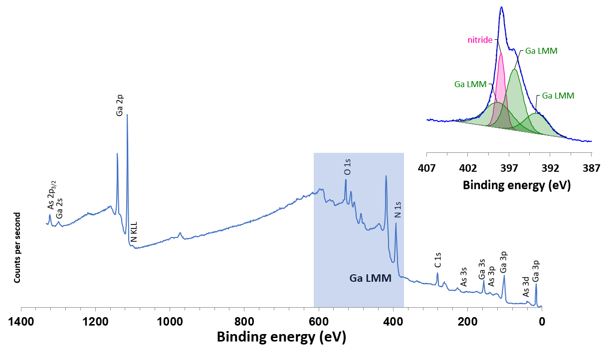
Figure 1. Al Kα excited survey spectrum from GaAs1-xNx and (inset) N 1s/Ga LMM region high resolution scan. Image Credit: Kratos Analytical, Ltd.
The N 1s/Ga LMM envelope gives rise to a broad, complex structure. A single symmetrical component is used for the N 1s peak, with three broad peaks used to characterize the Ga LMM transitions.
Whilst the model fits the data well, with such a great number of components, it is possible that there is not a singular fit that describes this envelope appropriately. This is a complex issue when the nitrogen concentration and chemical state are of critical importance for the performance of the material.
In contrast to the photoemission process, it is understood that the kinetic energy of the Auger electron is defined by the energy levels of the transitions involved in the Auger process and is independent of the energy of the excitation source used.
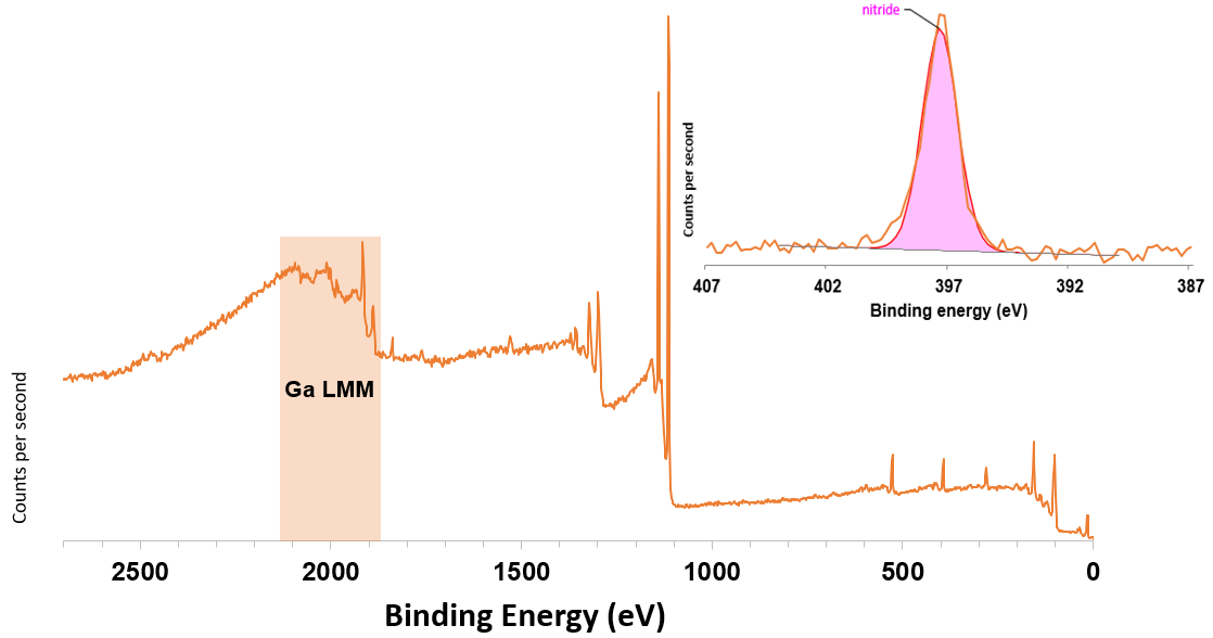
Figure 2. Ag Lα excited survey spectrum from GaAs1-xNx and (inset) N 1s region high resolution scan. Image Credit: Kratos Analytical, Ltd.
Figure 2 displays the survey spectrum from the same GaAs1-xNx sample excited utilizing the monochromatic Ag Lα excitation source.
It is apparent that the Ga LMM Auger transitions excited using the Ag Lα excitation apprently shifts them to higher binding energy so that they no longer overlap with the N 1s photoemission peak, as displayed in the inset high-resolution N 1s core level peak inset in figure 2.
The Ag Lα excited N 1s region offers a spectrum that is much more straightforward, with a single symmetrical peak centered at 397.6 eV. This is allows identification of nitrogen in a nitride-like chemical environment.
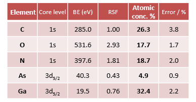
Eliminating the Auger transitions makes quantification of the survey spectrum easier. The relative elemental concentration of the elements is shown in table 1.
Table 1. Relative atomic concentrations of thin-film GaAs1-xNx on GaAs substrate from Ag Lα excited survey spectrum. Source: Kratos Analytical, Ltd.
It is interesting to comment further on the relative intensities of the photoemission peaks and change in sampling depths for core levels excited with the different X-ray sources in respect to the representation of the GaAs1-xNx thin film.
It is known that the photoionization cross sections for core level spectra decrease in response to an increase of excitation energy.2,3 This can be seen in figure 4 by the plot of C 1s photoionization cross section in relation to Al Kα excitation plotted as a function of excitation energy.
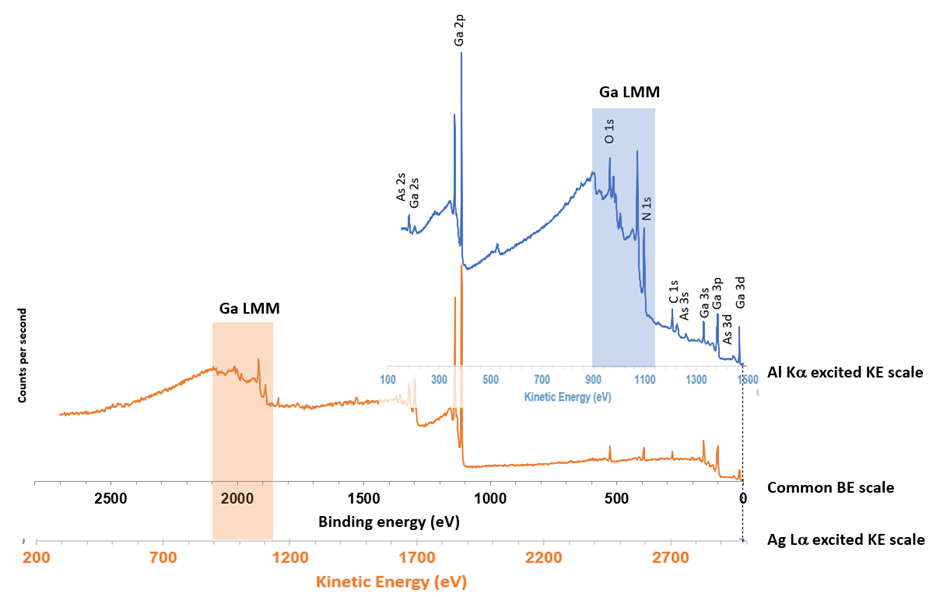
Figure 3. Overlay of Al Kα and Ag Lα excited spectra with both binding and kinetic energy scales. The two survey spectra were normalized to the Ga 2p3/2 peak height. Image Credit: Kratos Analytical, Ltd.
It can also be qualitatively observed in the overlay survey spectra shown in figure 3.
When contrasting the relative intensities of the photoemission peaks at the low binding energy end of the spectra relative to the Ga 2p peaks in each spectrum, it is clear to see that the peaks in the Ag Lα excited spectrum are of diminished intensity when compared to those excited by the standard Al Kα source.
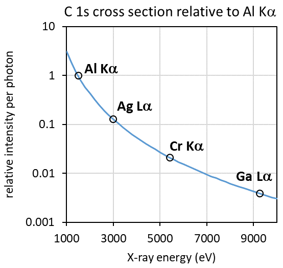
Figure 4. Calculated C 1s photoionization cross section plotted as a function of X-ray excitation energy, with commercially available HAXPES sources indicated. Image Credit: Kratos Analytical, Ltd.
As detailed in figure 4, the decrease in photoionization cross section would be considerably worse for the harder X-ray sources with greater energy, proving the benefit of the Ag Lα source for this study.
Contrasting the high resolution N 1s regions excited with the two X-ray sources, it is clear to see that a reduction in the photoionization cross section for the Ag Lα does not significantly impact the quality of the spectrum.
The efficient collection and transmission of the photoelectrons generated by the spectrometer design alleviates the physical effect of producing fewer photoelectrons. Ag Lα excited high resolution spectra are still acquired in sensible acquisition times, particularly when considering this sample’s relatively low dopant concentration of nitrogen in the thin film GaAs1-xNx.
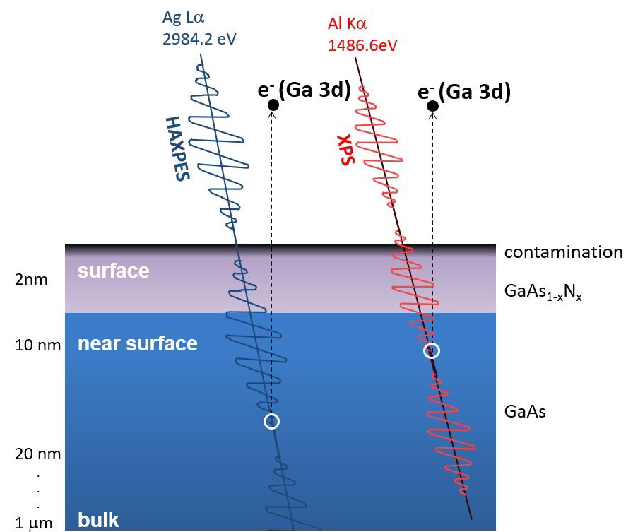
Figure 5. Schematic diagram of greater sampling depth for the same core-level excited with higher photon energy Ag Lα X-rays. Image Credit: Kratos Analytical, Ltd.
A major benefit of employing higher energy photon sources is the increased sampling depth due to the change in effective attenuation lengths of the higher kinetic energies of excited photoelectrons. This is schematically displayed in Figure 5.
The greater kinetic energy of the same core level photoelectron, when excited by the Ag X-rays in relation to Al X-rays, produces a greater information depth.
Qualitative and quantitative chemical state information can be derived as a function of depth without the necessity for angle-resolved XPS or destructive sputter depth profiling due to the fact that Ga and As 2s photoelectrons will demonstrate greater surface sensitivity than the higher kinetic energy 3d photoelectrons.
A final remark on quantification demonstrates that both the photoionization cross section and the sampling depth are key considerations in producing quantitative results from this sample which is inhomogeneous as a function of depth from the surface.
To produce a realistic quantification for the material, it is critical that the photoemission peaks selected for quantification possess as similar kinetic energies and, therefore, information depths as possible.
Conclusions
The Ag Lα excitation source was used to collect X-ray photoelectron spectra from a thin-film GaAs1-xNx grown on a GaAs substrate.
Utilizing the higher photon energy source has the considerable advantage that the Ga LMM Auger transitions overlapping with the N 1s photoemission peak - when using standard Al Kα excitation – are shifted to higher binding energy.
This enables an unambiguous curve fitting of a single N 1s component and classification of a nitride-like chemical state.
References
- A. Mascarenhas, Yong Zhang, "Electronic structure of nitrogen-doped GaAs and GaP," Proc. SPIE 10303, GalliumNitride-based Technologies: A Critical Review, 103030D (28 August 2002); https://doi.org/10.1117/12.482617
- Curran Kalha et al 2021 J. Phys.: Condens. Matter in press DOI: 10.1088/1361-648X/abeacd
- A. G. Shard et al., Surf. Interface Anal., 2019, 51, 763-773 DOI: 10.1002/sia.6647

This information has been sourced, reviewed and adapted from materials provided by Kratos Analytical, Ltd..
For more information on this source, please visit Kratos Analytical, Ltd..