A significant portion of semiconductor devices currently in production are classified as light-emitting diodes (LEDs).
LEDs are the light of choice when it comes to most lighting applications, both for the more conventional use as room lights but also for newer display technologies, including HD televisions, smartphones and augmented reality headsets.
With a ~10% higher efficiency and ~3x longer lifespan than compact fluorescent light bulbs, this popularity is no surprise; moreover, the devices are fast, small, and directly addressable.
The process of manufacturing μLEDs and similar semiconductor devices can be multi-stage (often several hundred different steps) and the process can last for weeks.

Figure 1. Display devices employing μLEDs, including (left) LED television, (middle) augmented reality head-mounted display, and (right) smartphones. Image Credit: Gatan Inc.
Therefore, it is imperative to analyze and determine device viability during the process of fabrication in order to avoid processing defective or faulty devices any further, as well as to perform failure analysis (FA) to improve the throughput of future batches by optimizing processing steps.
Figure 2 depicts a simplified workflow for wafer-mounted μLEDs.

Figure 2. Flow chart illustrating device production for μLEDs presented. Image Credit: Gatan Inc.
Today, there remains a lack of non-destructive techniques for defect identification that can be used in between production steps to identify faults, such as electrical shorts, handling defects, dielectric layer faults or semiconductor composition metrology, despite the pressing need to increase μLED device yield.
However, the announcement from Monarc® of their cathodoluminescence (CL) detector for scanning electron microscopes (SEMs) is set to change that.
The new Monarc detector offers luminescence characterization from 6" wafer level to the nanoscale and provides the most accurate correlation with other signals.
Such a capability facilitates the simultaneous capture of topographical, compositional and crystallographic information, significantly improving failure analysis capabilities.
Methods
The light emitted from a sample excited with energetic electrons (otherwise known as CL) has demonstrated substantial value in the compound semiconductor industry in device characterization and process development and is a valuable tool in analyzing dielectric materials.

Figure 3. The Monarc CL detector is attached to a scanning electron microscope. Image Credit: Gatan Inc.
Material identification, which is not easily determined by conventional optical or SEM analysis, is facilitated by this spectroscopic analysis.1 A significant advantage of performing CL in an electron microscope is that the nanometer-sized analysis spot can assist in full-wafer inspection (and metrology) to characterize to the nanoscale of individual microLEDs.

Figure 4. A CL spectrum captured from rare-earth-doped ceramic, revealing emissions across the ultraviolet, visible, and near-infrared portions of the electromagnetic spectrum. Image Credit: Gatan Inc.
When it comes to determining the elemental composition with microscopic spatial resolution, energy dispersive spectroscopy (EDS) in the SEM is a key and critical technique. The use of the EDS technique in failure analysis (FA) is ideal as the technique offers analyses of the energy distribution of X-rays emitted from a sample.
From this information, the distribution of elements can be determined.
Results and Discussion
This work oversaw the analysis of commercially manufactured GaN-InxGa1-xN multiple quanta well (MQW) based miniLEDs fabricated on a 4-inch sapphire substrate using the Gatan Monarc CL and EDAX Octane Elite EDS systems, both of which were attached to an FE-SEM.
As depicted by Figure 5, each rectangular LED (Figure 5) was comprised of a stack of materials grown and selectively etched in sequence. These included – from the bottom up – a thin AlN buffer layer, ~2 μm of n-GaN, ~2 μm of Si-doped N+-GaN, 200 nm of MQW layers, 300 nm of Mg-doped P-GaN, 100 nm of indium tin oxide (ITO), coated with ~300 nm of SiO2 and metal contacts.

Figure 5. (left) Low magnification view of a partially completed LED wafer. (middle) Secondary electron image of a single LED. (right) Cross-section schematic of InGaN/GaN MQW LED. Image Credit: Gatan Inc.
While excellent for displaying surface morphology, the SEM image notably lacks information regarding the presence and consistency of both LED material distribution and defects.
The analysis of LED devices was performed by CL imaging, which revealed several defects used for FA to evaluate handling induced damage, material composition and fabrication defects.
Handling-Induced Defect
As displayed in Figure 6, secondary electron and unfiltered CL images were captured over a large area (~16 mm2). The CL image revealed low brightness in ~1% of LEDs exhibit low brightness - a defect that the corresponding SEM images did not identify.

Figure 6. (left) Secondary electron and (right) CL image of mini-LED array. CL image reveals a series of defected LEDs in the shape of an ‘x’ with reduced intensity. Image Credit: Gatan Inc.
The affected devices appeared in an 'X' pattern which notably did not correspond to the device column and row pattern. It was determined that this defect was likely caused by mishandling during the process of fabrication.
To determine the defect's source and whether the devices remained viable for implementation, these defective devices were investigated further.
As shown in Figure 7, a CL spectrum image (hyperspectral map) was taken for one of the defective LEDs (yellow box). The CL maps indicate a surface influence primarily affecting the MQW layer emission, a mechanical scratch, which was likely introduced after the MQW but before metal deposition.
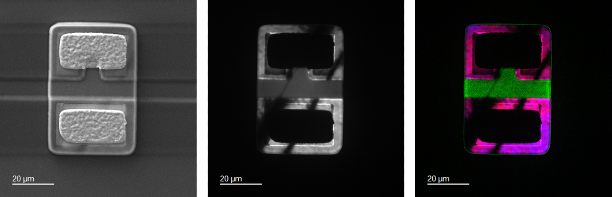
Figure 7. (left) Secondary electron image, (center) CL spectrum image displaying wavelengths from 300 – 700 nm, and (right) colorized spectrum image highlighting emission from GaN (360 nm, green colorization), and InxGa1-xN (430 nm, blue colorization; and 460 nm, red colorization) with 20 nm bandwidth. Each color band is normalized by intensity. Image Credit: Gatan Inc.
It is likely that these defects compromised the electrical pathways, and thus, LED light emission would be significantly reduced or circumvented. As a result, it was determined that they should be rejected from further processing.
Through the use of CL, it is possible to determine which devices are compromised, and a map may be generated to allow users to selectively exclude defected devices from further processing.
Defects like these can cause the exclusion of large regions of wafer area, supporting dozens of devices. Such defects are generally the most easily avoided, given that they originate from human interactions – for instance, during the exchange between instruments during processing or wafer transport.
Electrical Defect
Unfortunately, packaged device performance degradation is just one of an entire array of issues that can result from defects affecting the electrical connections in LEDs. The most common electrical defects include open circuit and short circuit.
As Figure 8 depicts, a number of LEDs were observed with missing metal contact pads, a defect that leads to a device that may behave as an open circuit electrically. Thanks to the bright regions in the CL image where the metal layers should have been, the missing contact pads were easily located.
The CL brightness was 2.5x brighter than areas with cladding due to the absence of the cladding layers.

Figure 8. (left) Secondary electron and (right) unfiltered CL images of LEDs with missing metal contact pads. Image Credit: Gatan Inc.
Figure 9 shows an LED with an electrical short defect. Such defects are fatal, given that they prevent LED functionality and can additionally lead to power loss.
The contacting material casts a dark shadow and demonstrates a bright-to-dark contrast ratio of up to 7:1 with the surrounding region. For the secondary electron image, the contrast ratio is only 2:1.

Figure 9. (left) Secondary electron image and (right) corresponding CL image of an electrical short defected LED. Image Credit: Gatan Inc.
Observing CL images drastically simplifies the discovery of electrical short defects. The CL map provides an enhanced contrast which facilitates the design of more robust algorithms for automatic failure detection algorithms, which have a consequent increase in device yield.
Fabrication Defects
Several other defects were also revealed by CL mapping. These defects include fabrication defects in close proximity to the upper and lower device contacts, as depicted by Figure 10. CL, in this instance, did not provide a clear and definitive explanation as to the nature of the defect.
EDS mapping and CL imaging were performed simultaneously to determine the type of defect.
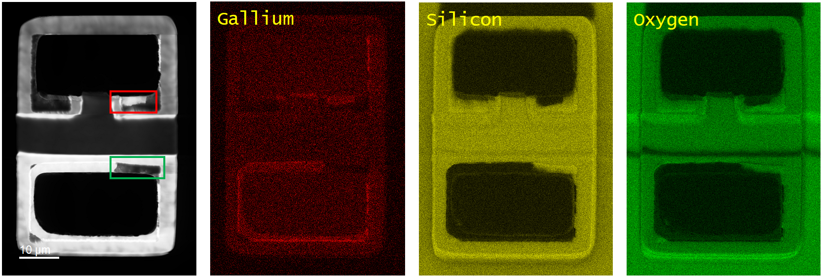
Figure 10. (left) Unfiltered CL image and EDS material composition results of a defect LED. EDS material mapping for gallium (red), silicon (yellow), and oxygen (green). Image Credit: Gatan Inc.
As shown in Figure 10, the EDS maps exposed local deficiencies in silicon and oxygen and excess gallium for the defects shown by the red box resulting from SiO2 being unintentionally removed during one of the liftoff processing stages; other areas (green box) revealed an excess of SiO2.
Material Composition
In Figure 11 (left), however, the CL image revealed a very strong emission intensity and showed some LED surface variation (which was not covered by opaque metal layers).
The center image in Figure 11 shows a spectrum image captured and colorized to reveal variance in the indium-fraction distribution of the LED MQW.

Figure 11. (left) CL spectrum image displaying wavelengths from 300 to 700 nm, (center) colorized spectrum image highlighting emission from GaN (360 nm, green colorization), and InxGa1-xN (430 nm, blue colorization; and 460 nm, red colorization) with 20 nm bandwidth. Each color band is normalized by intensity. (right) LED CL spectra from (red) MQW region and (blue) central GaN region (increased by a factor of 10 for clarity). Image Credit: Gatan Inc.
This central image in Figure 11 is comprised of three bandpass images that were extracted from the spectrum image, colorized and stacked together.
Emission at 430 nm is represented by the blue intensity, while 460nm comes from red and 360nm at the green (each with a 20-nm bandwidth). This composite bandpass image depicts areas where the red intensity is lesser, suggesting lower concentrations of indium locally by about 0.4% less than the average of 16.2% (In).
It must be noted that this variance is not substantial enough for it to be rejected from further processing.
Figure 11 (right) presents spectra extracted from the spectrum image, (red) from the MQW and (blue, x10) from the GaN region, which demonstrated a very strong intensity near 450 nm parallel to the InGaN emission and the GaN at 365 nm.
Summary and Conclusions
A significant amount of time and resources are needed for semiconductor device production. Therefore, metrology and inspection are essential to ensure that resource allocation is not wasted on devices that are defective.
CL provides invaluable inspection techniques with supplementary EDS, which facilitate direct observation of multiple defect types, which lead to a significant degradation in device performance.
Moreover, CL is able to image layers below the surface, which permits the determination of defect impact by measuring device intensity. This ability supports the development of more robust defect identification algorithms based on enhanced contrast.
EDS can thus detect forms of defects by determining the elemental composition of the defected areas.
References
- D. J. Stowe, J. D. Lee and M. Bertilson, "Octane Elite and Monarc Come Together to Capture EDS and CL Simultaneously," EDAX Insight, pp. 1-2, September 2020.

This information has been sourced, reviewed and adapted from materials provided by Gatan Inc.
For more information on this source, please visit Gatan Inc.