Modern Electron Backscattered Electron Diffraction (EBSD) detectors can quickly (in less than an ms) index a Kikuchi pattern, which is the diffraction pattern of crystalline materials in the SEM. With the help of an analytical SEM equipped with high probe currents, quality EBSD mappings can be efficiently recorded in just a few minutes.
However, the surface of crystalline materials is often not crystalline due to various factors such as atmospheric contamination, the growth of an amorphous oxide layer, and damage caused by the foregoing traditional mechanical preparation methods.
Broad Ion Beam (BIB) milling is a highly effective SEM sample preparation method that efficiently eliminates surface preparation artifacts and prepares the surface for the EBSD technique.
This article discusses the successful use of BIB with a Hitachi IM5000 for the EBSD analysis of a 2-phase as cast nickel base, both before and after BIB end polishing.
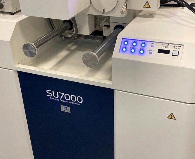
Image Credit: Hitachi High-Tech Europe
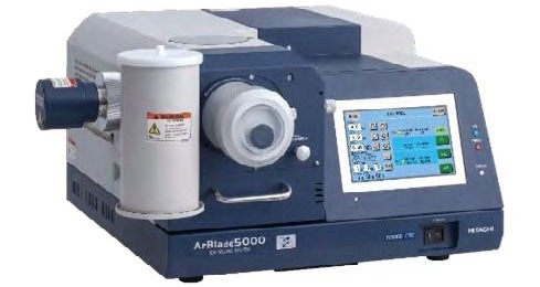
ArBlade5000 (Cold Trap was not used). Image Credit: Hitachi High-Tech Europe
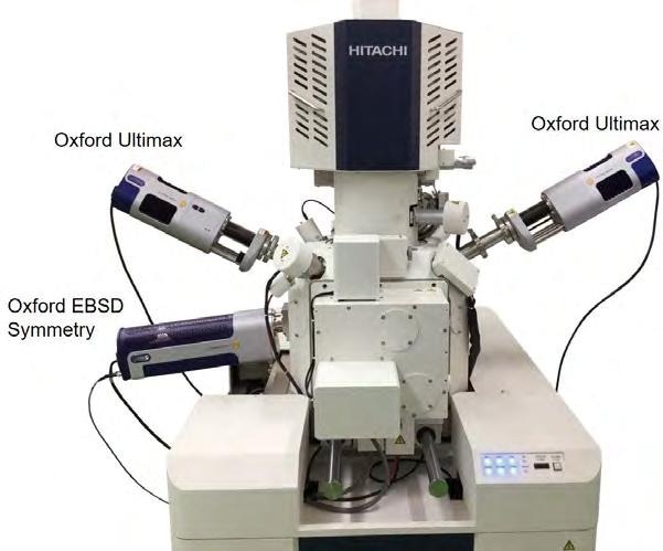
Hitachi SU7000 with Oxford EDX and EBSD. Image Credit: Hitachi High-Tech Europe
Instrumentation
The EBSD measurements were conducted on the High-Resolution Analytical VP SU7000 FE-SEM, equipped with an Oxford EDX (Ultim100), an EBSD detector (Symmetry), and the AZTEC operation software.
The SU7000 features a booster electron optics that operates within a wide range of electron voltages, from 10 eV to 30 kV. It is also equipped with a Hitachi Schottky Field Emission Gun, which enables probe currents of 200 nA in both High and Low Vacuum.
Three EBSD sample types are available for analysis in both High and Low Vacuum modes:
- 1st: Samples with heights up to 65 mm and more on a pretilted EBSD holder
- 2nd: Samples with a recommended height of 50 mm and diameter of 25 mm when utilizing the fully eucentric tilt function. This is perfect for automated low-magnification EBSD mappings that can be done overnight
- 3rd: TEM samples, prepared using methods such as electropolishing, ultra-microtome, or FIB-enabling Transmission Kikuchi Diffraction, TKD
The BIB preparation was carried out using the ArBlade5000 ion milling system, which operates with Ar from 0-8 kV and features a milling rate of 1 mm/hr or higher for Si.
The stage can be cooled to -100 °C for beam-sensitive samples using an LN cold trap. There are two operation modes available:
Cross-Section Milling
The sample is positioned between the mask and holder, with the Ti mask serving as a cutting edge.
Flat Milling
Where a conventionally prepared cross section is positioned on a rotational holder and meticulously polished using the argon beam at various angles.
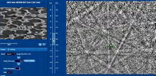
For this study, the Flat Milling mode was utilized in two steps with a stage tilt of 85°.
Step 1: Apply a voltage of 8 kV for 5 minutes
Step 2: Apply an additional 1.5 kV for five more minutes
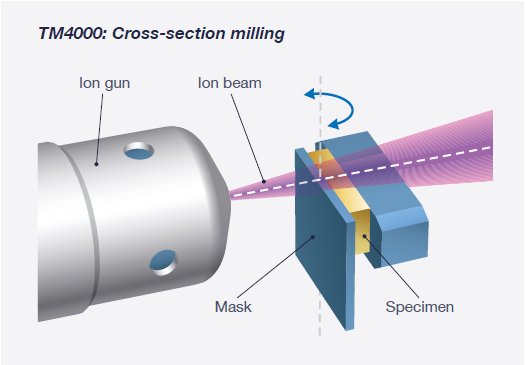
Image Credit: Hitachi High-Tech Europe
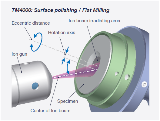
Image Credit: Hitachi High-Tech Europe
Image Credit: Hitachi High-Tech Europe
SEM and EDX Analysis
The sample, an as-cast NiAlTa alloy, has been prepared as an embedded cross-section with a diameter of 25 mm and polished both electrochemically and mechanically. The surface details and inner microstructural information were imaged simultaneously using the Upper, BSE, and EDX detectors at a WD of 6 mm and 30 kV.
Take note of the Mo-K line at 17.4 kV, respectively. The UD signal uncovers preparation artifacts caused by the mechanical preparation and surface contamination, while the BSE signal displays a microstructure consisting of two phases: a “bright” matrix phase and a dark “precipitation” phase containing particles as small as 100 nm.
When the same area was imaged and analyzed at 5 kV, the phase boundaries became much more distinct, and precipitations located deeper than the information depth were no longer visible. This is because the electron beam at 5 kV has a smaller penetration volume than 30 kV.
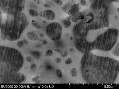
NiAlTa alloy imaged at 30 kV with the Upper Detector (UD). Image Credit: Hitachi High-Tech Europe
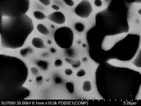
NiAlTa alloy imaged at 30 kV with the BSE detector (PDBSE(COMP)). Image Credit: Hitachi High-Tech Europe
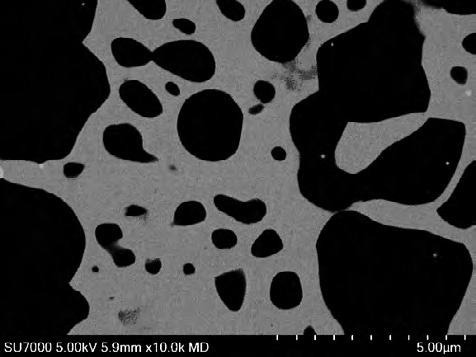
NiAlTa alloy imaged at 5 kV with the BSE detector (PDBSE(COMP)). Image Credit: Hitachi High-Tech Europe
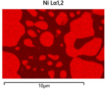
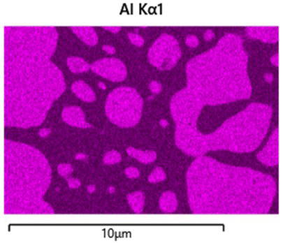
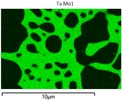
Based on the EDX mappings at 5 kV, the “bright phase” contains a significant amount of Ta, while the “dark phase” primarily consists of Ni and Al. During the dark phase, Ta-rich precipitations not visible in the 30 kV image can be identified. Additionally, an estimated lateral EDX resolution of 130 nm can be determined.
Analyzed using a 100 mm² EDX detector at 15 kV with a count rate of >400 kcps for 30 seconds, the average weight and the concentration of the two phases were determined.
A single average spectrum was recorded at low magnification and quantified in atomic percentage (at%). The phases were analyzed using five spot measurements under the given conditions and quantified using standard deviation.
Quantitative EDX measurements of the alloy and its two phases. Image Credit: Hitachi High-Tech Europe
Source: Hitachi High-Tech Europe
| |
Ni |
Al |
Ta |
| average (at%) |
19.67 |
50.04 |
30.29 |
| “bright“ Ni phase (at%) |
41.13
+/- 0.13 |
28.03
+/- 0.14 |
30.84
+/- 0.07 |
| “dark“ NiAl phase (at%) |
50.69
+/- 0.12 |
49.31
+/- 0.12 |
0.0
+/- 0 |
EBSD Analysis Before Flat Milling
During a 5-ms spot EBSD analysis, a Kikuchi pattern was observed in the NiAl phase, which the EBSD software was successfully identified as a NiAl phase. Several Ni and NiAl crystallographic references from the databases were identified. Spot analysis in the Ta-rich bright phase does not show any pattern.
Consequently, the dark phase can be accurately EBSD mapped with a high indexing ratio, while the bright phase has no viable solutions. The mapping below displays band contrast images, Euler color, and inverse pole figures. It was conducted at 20 kV, 4.6 nA, for four minutes.
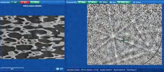
EBSD spot analysis before ion milling: A Kikuchi pattern can be found only in the dark phase (top image). Image Credit: Hitachi High-Tech Europe
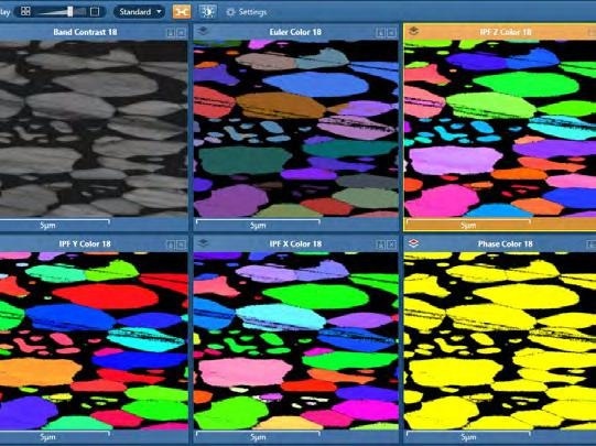
EBSD mapping before ion milling: Only the dark phase can be indexed. Image Credit: Hitachi High-Tech Europe
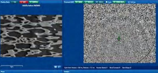
EBSD Analysis After Flat Milling, Step 1:
The sample was analyzed under identical conditions following a Flat Milling cycle at 8 kV for five minutes, yet no significant differences were observed.
EBSD spot analysis after 1.5 kV ion milling: Kikuchi patterns can now be found in both phases (top and bottom images). Image Credit: Hitachi High-Tech Europe
EBSD Analysis After Flat Milling, Step 2:
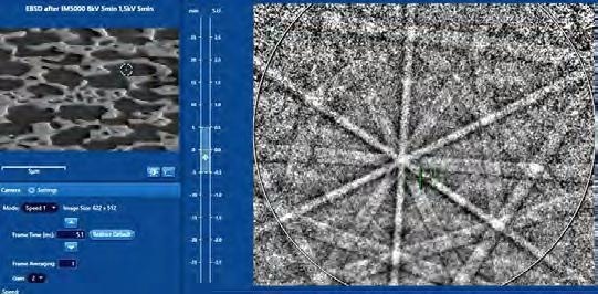
Another milling step was performed for five minutes at 1.5 kV, and similar areas of interest were chosen. During both phases, the quality of the Kikuchi pattern was noticeably enhanced, enabling EBSD mapping with high indexing ratios.
Therefore, both phases are associated with a high indexing ratio. The table below illustrates the distribution of different stages in the analyzed area. The majority, 63.03%, was identified as NiAl, followed by 36.78% as Ni, 1.23% as Zero solution, and 0.96 as a Ni3(Al0.5Si0.5) phase.
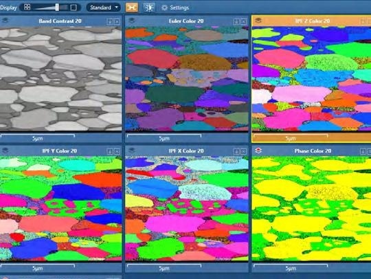
EBSD mapping after 1.5 kV ion milling: Both phases can be indexed. Image Credit: Hitachi High-Tech Europe
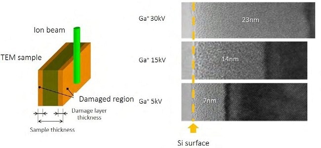
Influence of the Ga-ion energy on the damage of a Si lattice. Image Credit: Hitachi High-Tech Europe
Phases and their fractions found after 1.5 kV ion milling. Source: Hitachi High-Tech Europe
| Phase Name |
Phase Fraction |
Phase Count |
| Ni-superalloy |
0.00 |
0.00 |
| NiAl |
61.03 |
0.00 |
| Nickel |
0.00 |
103049 |
| Ni3(Al0.5Si0.5) |
0.96 |
0.00 |
| Ni |
36.78 |
63095 |
| Zero Solutions |
1.23 |
2081 |
Conclusion
This study demonstrates that using the Broad Ion Beam milling approach with Ar can greatly enhance the surface of crystalline materials, preparing them for EBSD analysis.
Nevertheless, the measurements suggest that choosing the appropriate ion milling kV is crucial. The 1.5 kV beam reveals the crystal character of the Ni phase, although it is not apparent with the 8 kV beam.
This behavior is commonly observed in Atomic Resolution Transmission Electron Microscopy: as the energy of ions used to prepare a TEM sample increases, the level of damage also increases, which can affect lattice resolution.
The image above displays the amorphization thickness of a Si-TEM lamella after following preparation with Ga ions at 30 kV, 15 kV, and 5 kV. The thickness decreases from 23 nm to 14 nm and further down to 7 nm.
Using a lower Ar beam energy of 1.5 kV should effectively eliminate any amorphous contamination or damaged surface layers, resulting in a higher success rate for generating EBSD patterns.

This information has been sourced, reviewed and adapted from materials provided by Hitachi High-Tech Europe.
For more information on this source, please visit Hitachi High-Tech Europe.