As semiconductor devices increase in both size and complexity, nanometer-scale metrology has become crucial. While conventional atomic force microscopy (AFM) excels at delivering high-resolution outcomes, it generally only covers areas up to approximately 100 x 100 μm.
Bruker’s Large-Area Scanning and exclusive, patented HyperMap™ technologies are capable of far surpassing this field-of-view limitation, bridging the gap between localized AFM precision and wafer-scale process control.
This article details the operating principles of Large-Area Scanning and HyperMap, followed by case studies demonstrating full-die topography data collection via Large-Area Scanning and hotspot inspection using HyperMap.
Why Is Large-Area Metrology Crucial for CMP and Bonding Performance?
Large-Area Scanning and HyperMap on InSight® AFP-HB (Figure 1) allow semiconductor producers to maintain high vertical and planar resolution while capturing long-wavelength fluctuations across larger areas, such as an entire die.
Topographic variations at these larger millimeter scales can substantially affect chemical mechanical planarization (CMP) procedures, as well as hybrid bonding, lithography, and packaging.
Recent studies have shown that within-die non-uniformity (WiDNU), pattern density dependencies, and long-range planarity issues are becoming increasingly difficult to address, particularly as die sizes approach 800 mm2 and beyond.1,2
These topographical inconsistencies manifest as dishing, erosion, and surface topography variations that compromise device yield and bonding integrity. Hybrid bonding is especially sensitive to such topographical defects, meaning it requires ultra-flat surfaces across both copper (Cu) and dielectric regions at the local scale, along with planarity over millimeter-scale lateral distances within a die.
Coupling nanometer-scale vertical resolution with millimeter-scale lateral coverage provides the metrology capacity necessary to characterize and manage these multi-scale topography difficulties.
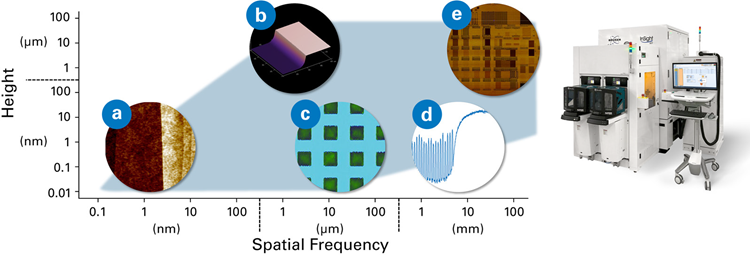
Figure 1. Map representing the field of view, spatial frequencies, and height ranges covered by InSight AFP-HB. Examples are shown for (a) atomic steps on 2D material, (b) 10 μm step height, (c) 100 μm bond pad metrology scan, (d) 20 mm profile scan, and (e) 22 mm large-area scan of a full die. Image Credit: Bruker Nano Surfaces and Metrology
White light interferometry (WLI) has historically been used to perform post-CMP hotspot inspection. Though effective in certain applications, this method is limited by material dependencies, typically requiring a reflective coating to prevent artifacts that arise when dissimilar materials are present.
For this reason, wafers must be removed from the manufacturing flow, coated, and then inspected. This results in substantial delays and sacrifices valuable product wafers for each measurement.
This metrology loop affects throughput while introducing uncertainty and cost, driving the need for a faster, non-destructive alternative capable of operating in-line and at manufacturing speed.3
Large-Area Scanning and HyperMap technologies allow for in-line, non-destructive nanoscale topography mapping across full-die and multi-die regions. These techniques bridge the gap between localized AFM precision and wafer-scale process control, providing producers with instruments to detect, understand, and mitigate millimeter-scale CMP-induced variations.
Addressing Traditional AFM Scan-Range Constraints
Typical lateral (XY) AFM mode scan ranges for InSight AFP-HB span from hundreds of nanometers to 105 x 105 μm. To cover larger fields of view, one of two strategies can be deployed:
- Multiple images are collected and stitched together, though this method is time-intensive and compromises throughput.
- A rapid, high-precision stage is used to raster-scan the sample beneath a stationary probe. This approach expands the accessible scan area to match the available travel range of the stage, even providing full coverage of a 300 mm wafer surface. The map in Figure 1 illustrates the field of view, spatial frequencies, and height ranges covered by InSight AFP-HB using this technique.
Bruker, alternatively, has two advanced techniques for conducting large-area AFM metrology: Large-Area Scanning and HyperMap.
Large-Area Scanning for Unprecedented Lateral Coverage
Large-Area Scanning can be conceptualized as a high-precision, large-scale implementation of AFM, essentially a scanning-sample AFM setup that allows for unprecedented lateral coverage.
During a large-area scan, a precision air bearing stage is used to raster-scan the sample beneath a stationary probe. Concurrently, the Z-piezo actuator maintains closed-loop feedback to monitor surface height through standard AFM feedback mechanisms.
The probe functions in oscillatory feedback mode, similar to traditional TappingMode AFM. As the sample moves beneath the probe, surface height variations modulate the oscillation amplitude, which maintains tip-sample interaction and reconstructs the topography with nanometer-scale resolution.
Additional features of Large-Area Scanning that enable precise, dependable metrology are:
Continuous scanning: Scanning is performed as a single, uninterrupted procedure. Retracting the probe between scan lines disrupts measurement continuity and impairs spatial registration between lines.
Reference-plane acquisition: A low-resolution reference scan is carried out before the high-resolution scan. This reference serves as a baseline for post-acquisition leveling, guaranteeing that the final topography data is free from stage-induced tilt or drift.
Feedback dynamics optimized for scale and throughput: While similar to conventional TappingMode AFM, the closed-loop feedback dynamics are optimized for throughput across the larger length scales of Large-Area Scanning, in conjunction with application-specific probe designs.
Collectively, these design principles enable InSight AFP-HB to provide high-resolution, large-scale topography maps that are crucial for advanced semiconductor process control, particularly in applications such as CMP characterization and lithography alignment.
It should be noted that the vertical resolution of large-area scans remains equivalent to that of standard AFM, maintaining nanometer-scale sensitivity. Lateral resolution is user-configurable and is typically optimized according to throughput and application-specific requirements.
Figure 2 presents an example of Large-Area Scanning on a commercially available metrology test wafer (AMAG7).4 The 7 x 7 mm scan is composed of 700 lines and 8412 pixels per line. Line sections at several selected positions (Figure 2b) demonstrate the ability to track subtle height variation across large areas.
Figure 2c depicts a digital zoom of a 1 x 1 mm area, demonstrating good correlation with a separate (traditional) 100 x 50 μm AFM scan of the same area, as shown by the images and section profiles in Figures 2d and 2e.
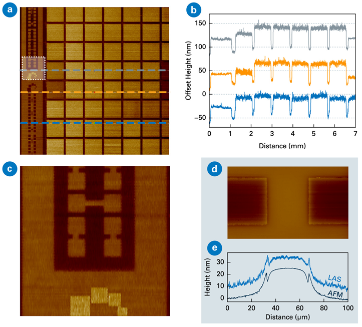
Figure 2. Example large-area scan on a commercially available AMAG7 Metrology Test Wafer, with comparison to conventional AFM scan. (a) 7 x 7 mm Large-Area Scanning image, (b) section profiles in three positions, and (c) digital zoom to a 1 x 1 mm area, (d) 100 x 50 μm conventional AFM scan of the same area, and (e) single-line section profiles from both (c) and (d), illustrating how Large-Area Scanning width and height metrology data matches conventional AFM. Image Credit: Bruker Nano Surfaces and Metrology
Balancing Coverage, Resolution, and Throughput with Large-Area Scanning
Thanks to its versatile options for adjusting scan area, resolution, and acquisition time, Large-Area Scanning is well-suited to a wide range of semiconductor metrology applications in both process development and high-volume manufacturing (HVM). These include CMP process monitoring and lithography focus control.
In process control applications, nanoscale topography over millimeter-length scales can mean the difference between yield, rework, or scrap. In many of these situations, ultra-high lateral resolution is unnecessary, and a lower-resolution scan can be completed within minutes, delivering adequate metrology for fast process decisions.
Alternatively, certain applications require detection of localized surface characteristics, such as wiring-density-induced hotspots or defect clusters. These scenarios demand increased lateral resolution, whereas acquisition time may be a secondary consideration.
InSight AFP-HB addresses these requirements by supporting submicron line spacing, enabling in-depth characterization of small-scale features.
Large-Area Scanning Case Study: Hybrid Bonding
A second example, directly tied to a real-world wafer-to-wafer hybrid bonding challenge, is depicted in Figure 3. Post-bonding inspection employing confocal scanning acoustic microscopy (CSAM) identified persistent multimillimeter-scale voids between bonded wafers. Since these defects were only detectable after the wafers had been permanently joined, corrective action was impossible, resulting in costly wafer loss.
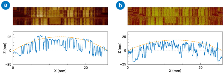
Figure 3. Large-area scans of the same 26 x 5 mm wafer area (a) before and (b) after topography fabrication mitigation techniques. Image Credit: Bruker Nano Surfaces and Metrology
Scanning the full 26 x 33 mm die via Large-Area Scanning revealed that areas with elevated topography correlated to variations in underlying layer density, which were the root cause of bonding voids.
With this insight, the device producer isolated a crucial region of interest and decreased the scan area to a targeted 18 x 6 mm region, allowing for more rapid acquisition times and making it practical to incorporate Large-Area Scanning into the routine manufacturing monitoring cycle.
Figures 3a and b illustrate the same region, imaged using the same recipe, scanned before and after the CMP process enhancement. The change yielded a measurable reduction in long-range topography from 25 nm to 15 nm.
The topography data generated by Large-Area Scanning enabled the manufacturer to tune their CMP process, reducing excess topography and considerably enhancing both bonding quality and device yield.
Today, Large-Area Scanning is a standard component of the company's post-CMP metrology workflow, ensuring surface planarity before wafer bonding and supporting powerful hybrid bonding performance.
HyperMap for Highest Data Acquisition Speeds
HyperMap is optimized for high-speed data collection in HVM. It is a robust instrument for rapid, non-destructive, in-line topography inspection and metrology of CMP-induced surface variations across crucial wafer areas.
Although HyperMap shares foundational principles with Large-Area Scanning, it is a distinct technology that uses Bruker’s proprietary and patented detection technology to allow for ultra-high scan rates of up to tens of millimeters per second.5
Originally developed as an inspection mode for determining single-micron scale (XY) post-CMP hotspots across full-field sizes (26 x 33 mm), HyperMap has evolved alongside the increasing implementation of hybrid metrology in HVM. It is now a metrology-grade solution for topographical review that offers an attractive alternative to conventional Large-Area Scanning when speed is crucial.
Currently, HyperMap is most commonly employed to scan targeted regions of interest (often several millimeters in size) where topographic variations caused by wiring concentration may affect downstream procedures, such as bonding.
Its high-speed acquisition ability has significantly shortened overall move-acquire-measure (MAM) time, decreasing it from several hours to less than one hour, without impairing vertical resolution.
When inspection-identified hotspots require additional, higher-resolution AFM metrology, Bruker’s Defect Review capability on the InSight platforms can facilitate nanometer-scale topographical and material metrology at targeted locations.
Enabling In-Line, Production-Scale Inspection with HyperMap
Conventional techniques, including WLI, remain important, but they frequently require pre-inspection wafer processing. Such processing takes time off the line and can lead to relaxation, resulting in wafers that may not accurately reflect the in-line morphology.
Similarly, the need for pre-inspection processing results in limited sampling that may not completely represent all wafers in the lot or run. Following inspection, processed and inspected wafers must be scrapped.
HyperMap, alternatively, is a non-destructive method that requires no pre-inspection processing. Eliminating this step enables quick inspection before relaxation can change the true nature of hotspots.
This strategy further supports larger sample sizes, providing a more comprehensive understanding of all wafers in the lot or run. Following inspection, the wafers may be returned to the line, redirected for additional metrology, or sent for rework.
Figure 4 depicts a HyperMap example on a 26 x 30 mm region of the AMAG7 wafer presented in Figure 2. The data was acquired in approximately two hours. Section profiles obtained from two areas demonstrate the ability to resolve nanoscale variations.
A digital zoom of the HyperMap section profiles is compared to a section profile acquired from a traditional AFM scan (Figure 4d) in one of the regions containing a dense line pattern. This comparison illustrates good correlation within the limitations of the pixel sizes used.
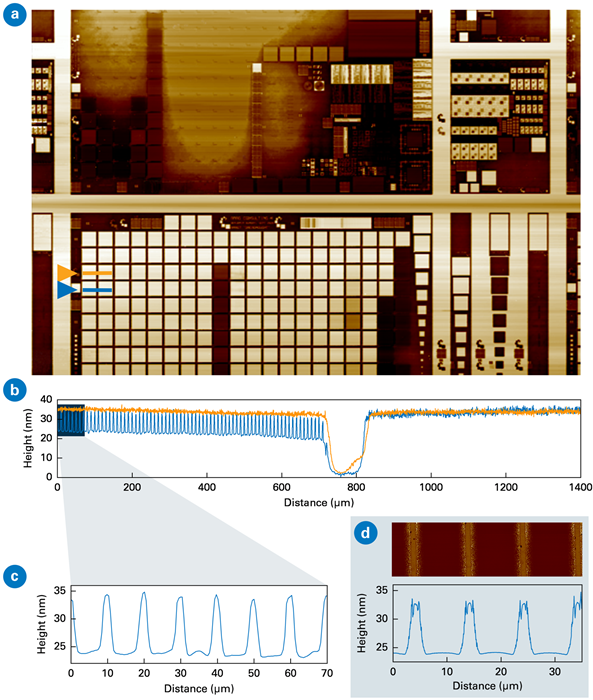
Figure 4. (a) 26 x 30 mm HyperMap scan, with (b) average section profiles in two areas, and (c) digital zoom into the data. (d) 35 x 10 μm high-resolution AFM scan with corresponding average section profile. Image Credit: Bruker Nano Surfaces and Metrology
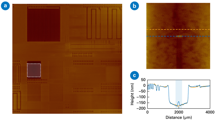
Figure 5. (a) 10 x 10 mm Hypermap with 1 x 1 μm pixel size, and (b) 1.2 x 1.2 mm digital zoom around the hotspot location located in the lowest part of the large scan. (c) A section profile through the hotspot is compared to a section profile taken from an adjacent location. Image Credit: Bruker Nano Surfaces and Metrology
HyperMap Case Study: Post-CMP Hotspots
Figure 5 presents an example of hotspot inspection using HyperMap. Post-CMP hotspots are surface anomalies that can impact device performance and yield. Early hotspot detection helps manufacturers adjust process parameters, prevent defects, and maintain the tight tolerances required for advanced nodes (which feature lateral dimensions up to approximately 5 μm).
Hotspots are often defined as localized regions where the surface height deviates beyond a specific threshold, usually 10–20 nm from the average surface level.
Large-Area Scanning and HyperMap Provide High-Throughput AFM Metrology for Full-Die and In-Line Inspection
Although AFM is a longstanding part of in-line semiconductor metrology, contemporary device architectures require nanoscale topography measurements across much larger regions than traditional AFM can efficiently cover.
Bruker’s Large-Area Scanning and HyperMap technologies address this challenge by allowing precise, repeatable metrology from the sub-micron scale to full-die dimensions.
These capabilities support crucial production stages, including CMP optimization and hybrid bonding process control. On InSight AFP-HB, dependable large-area AFM metrology is facilitated by custom-made instrument properties that maintain measurement integrity as scan speeds and dimensions increase, including:
- Artifact-free stage motion over large areas is provided by a dedicated air-bearing stage that reduces out-of-plane motion while maintaining low noise at elevated scan rates.
- Rapid, multi-directional scanning capability supports both raster scans and radial mapping approaches for versatile, process-driven workflows.
- An ultra-flat chuck with optimized wafer mounting maintains true surface topography across millimeter-scale and full-die scans.
Combined, these platform-level design features enable producers to employ Large-Area Scanning for in-depth, high-fidelity full-die metrology, and HyperMap for fast, in-line inspection of crucial areas without impairing vertical resolution or throughput.
By introducing non-destructive, production-scale AFM metrology earlier in the workflow, InSight AFP-HB helps detect topography-related risks before they can impact yield.
As CMP and hybrid bonding criteria continue to tighten, Large-Area Scanning and HyperMap offer a scalable, production-ready solution for faster feedback, enhanced process control, and more powerful device manufacturing performance.
Acknowledgments
Produced from materials originally authored by Sean Hand, Senior Staff Applications Scientist, Jorge Olivares Rodriguez, PhD, Applications, Scientist, YangYang Chen, PhD, Applications Engineer, Peter De Wolf, PhD, Senior Director of Technology and Application Development, all from Bruker.
References and Further Reading:
- Peters, L. (2023). Gearing Up For Hybrid Bonding. Semiconductor Engineering. Available at: https://semiengineering.com/gearing-up-for-hybrid-bonding/.
- Meixner, A. (2024). Precise Control Needed For Copper Plating And CMP. Semiconductor Engineering. Available at: https://semiengineering.com/precise-control-of-copper-plating-and-cmp/.
- Ervin, J. (2016). Pattern Dependence Process Modeling. Semiconductor Engineering. Available at: https://semiengineering.com/pattern-dependence-process-modeling/.
- Bunday, B.D. (2022). Metrology test artifact availability improvement. Metrology, Inspection, and Process Control XXXVI, p.70. DOI: 10.1117/12.2615726. https://www.spiedigitallibrary.org/conference-proceedings-of-spie/12053/2615726/Metrology-test-artifact-availability-improvement/10.1117/12.2615726.full.
- Osborne, J., et al. (2019). US10969406B2 - High speed atomic force profilometry of large areas - Google Patents. Available at: https://patents.google.com/patent/US10969406B2.
- Hand, S., and De Wolf, P. 2024. "Hybrid Bonding Surface Inspection Using InSight AFP-HB and AFM". Bruker Application Note AN5001.

This information has been sourced, reviewed, and adapted from materials provided by Bruker Nano Surfaces and Metrology.
For more information on this source, please visit Bruker Nano Surfaces and Metrology.